 All RF Cafe Quizzes make great fodder for
employment interviews for technicians or engineers - particularly those who are
fresh out of school or are relatively new to the work world. Come to think of it,
they would make equally excellent study material for the same persons who are going
to be interviewed for a job. Bonne chance, Viel Glück, がんばろう,
buena suerte, удачи, in bocca al lupo, 행운을 빕니다,
ádh mór, בהצלחה, lykke til, 祝你好運.
Well, you know what I mean: Good luck! All RF Cafe Quizzes make great fodder for
employment interviews for technicians or engineers - particularly those who are
fresh out of school or are relatively new to the work world. Come to think of it,
they would make equally excellent study material for the same persons who are going
to be interviewed for a job. Bonne chance, Viel Glück, がんばろう,
buena suerte, удачи, in bocca al lupo, 행운을 빕니다,
ádh mór, בהצלחה, lykke til, 祝你好運.
Well, you know what I mean: Good luck!
Click here for the complete list of
RF Cafe Quizzes.
Note: Some material based on books have quoted passages.
Return to RF Cafe Quiz #26
 This quiz
is based on the information presented in Substrate Noise Coupling in Analog/RF Circuits,
by Stephane Bronkers, Geert Van der Plas, Gerd Vandersteen, and Yves Rolain. Published
by Artech House. This quiz
is based on the information presented in Substrate Noise Coupling in Analog/RF Circuits,
by Stephane Bronkers, Geert Van der Plas, Gerd Vandersteen, and Yves Rolain. Published
by Artech House.
Note: Some of these books
are available as prizes in the monthly RF Cafe Giveaway.
1. Which is NOT a class of substrate noise analysis?
 d) Transverse d) Transverse
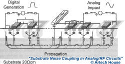
Figure 1.1, on page 3, illustrates generation, propagation, and impact substrate
noise analysis partitioning.
2. What is the most popular and straightforward method
for shielding analog integrated circuits against substrate
noise?
b) Guard rings
Per page 39, "Guard rings are passive isolation structures, which prevent substrate
noise currents from reaching the analog circuitry."
3. Aggressor and victim refer to what process?
b) The source of and recipient of substrate noise, respectively An aggressor
is the area of the substrate generating the potential noise source, and the victim is
the area to which the noise is coupled. See Figure 3.3 on page 41.
4. What is the best way to separate substrate coupling
noise from other regional noise coupling sources when developing mixed (digital/analog)
signal devices?
a) Dice between the regions to physically separate the digital/analog regions,
then wire bond between
During the development/characterization process, a dicing line can be designed into
the die that allows physically separating the two (or more) partitions, then wire bonding
between regions after mounting to a carrier. Wire bond lengths can usually be kept short
enough to not degrade function, but still permit determination of substrate noise sources.
See page 145.
5. At high frequencies, which off-chip noise coupling mechanism
typically dominates?
d) Magnetic coupling between die bond wires
Magnetic coupling between the die bond wires is typically many decibels greater than
PCB trace coupling. See page 142.
6. What is the primary source of FM modulated noise spurs?
c) Perturbations on the ground interconnect
"To reduce the power of the FM modulated spurs, the impedance of the on-chip ground
interconnect has to be small compared to the impedance of the PCB ground network." See
page 174.
7. In a VCO circuit, what is a likely mechanism for AM spur
generation and intermediate frequencies? a) Capacitive coupling from on-chip
inductors to the substrate
Parasitic capacitance permits the AM coupling by altering the reference potential
of the substrate. See page 175.
8. How are digital and analog grounds kept separate on the
die?
d) Separate digital / analog ground metal on the die, with separate off-chip
digital / analog grounding points As with PCB design,
maintaining isolated digital / analog grounds( and supplies when practical) is the best
method for avoiding coupling noise. Inserting a small value resistor (0.5 ohms) between
the PCB ground and the IC mounting pad can help reduce ground reference bounce. See page
186.
9. For what purpose is parasitic extraction used?
c) Obtaining parasitic RLC values for use in simulation In order to allow
more accurate simulation of devices, it is necessary to construct a robust equivalent
circuit model that includes intentional and unintentional R,L, and C values. The model
can then be used with high confidence in other designs. See page 200.
10. What determines to a large extent the efficiency of a P+
guard ring?
a) Impedance of the ground interconnect Substrate currents are picked
up by the P+ region of the guard ring and are drained toward the PCB ground.
See page 65.
|