
You are welcome to submit yours.
RF Cafe website visitor Ray
Gutierrez generously provided a paper for publication a few years ago, and now has
provided a follow-on article on the subject of intermod cancellation in RF amplifiers.
Says Ray, "This paper is a continuation work for the "New High Efficiency Intermodulation Cancellation Technique for Single
Stage Amplifiers." Published in January 2008 on RF Café's Paper section. The
paper describes configurations for dual and multiple parallel amplifiers and uses
the basic Reflect Forward technique for intermodulation cancellation. Some new improvements
were made to the RFAL technique to improve the efficiency and operation." Further,
"I had done much of the work for this new paper back then but got busy doing other
things in my retirement time. The other day I got back to it and figured it was
a shame to throw it all out without publishing it so that others may benefit. I
do not know if anyone has used this technique in a real product. I did not renew
the USA patent so anyone is now free to use it." Ray's paper is presented here in
HTML format, but at the bottom of the page is a link to the PDF file is you need
that.
Title: Reflect Forward Linearizer for Combined Amplifiers.
Author: R. Gutierrez
Date: February 2012
2/19/12 8:05 PM
Introduction: The new circuit configurations use the basic concept
of the published Reflect Forward (RFAL) intermodulation linearizer technique listed
in the references. The circuits use an improved fundamental signal cancellation
loop for significant input signal reduction in the composite IM error signal. The
vectored IM error signal improves the two-tone linearity of the system up to the
1 dB compression point of the combined amplifiers by (Intermod Loop ON/OFF delta
improvement of IMD3 >20 dBc). Two configurations are shown. One uses directional
couplers and the other circulators to sample the input reflected signals used for
intermodulation cancellation at the output of the combined amplifiers. The new circuit
can use more economical lower power dissipation components for higher power added
efficiency than previous configurations. The technique is applicable from single
to multiple numbers of parallel combined single stage amplifiers.
The basic RFAL technique uses the behavior of transistors when driven into its
non-linear operating region. At the high drive levels the input of the transistor
reflects not only the fundamental frequency components of the input signals but
also the non-linear distortion components that appear at the output of the transistor.
The level of the distortion products at the input are sufficiently proportional
to the output such that it can be used and processed as a correction or error signal
to cancel the output distortion of the main transistor amplifiers. The circuit samples
the forward and reflected signals from the amplifiers adjusting its phase and amplitude
to produce an efficient IM error cancellation signal that has a low level input
carrier content.
The basic block diagrams for the Parallel Combined RFAL (PC-RFAL) are shown in
Figure 1a and 1b.
References:
US Patent 6,573,793 "Reflect Forward Adaptive Linearizer" June 3 2003.
"The RFAL Technique for Cancellation of Distortion in Power Amplifiers", High
Frequency Electronics, June 2004.
"High Frequency Linearized LDMOS Amplifiers Utilize the RFAL Architecture." High
Frequency Electronics, February 2006.
"Criss-Cross RFAL Cancels the IMD Distortion in Amplifiers" December 2007. RF
Cafe website. Papers section.
‘New High Efficiency Intermodulation Cancellation Technique for Single Stage
Amplifiers" January 2008. RF Cafe website. Papers section.
Discussion for each of the main functional circuit blocks:
(Reference Fig 1a and 1b)
Combined Main Amplifiers
The two main amplifiers should be very equal in performance. The input of each
amplifier should be well matched, flat and smooth with no inflection points over
the operating band. The transistors can be GaAs or LDMOS type and DC biased Class
A or Class AB. Connections from the input couplers or circulators to the transistor's
input matching network should be kept short as possible since the added delay will
have to be compensated after the output of the main amplifiers and will add to the
output loss of the system.
Transistor selection for optimum IMD cancellation should be made with consideration
for linearity, cost, efficiency, frequency and power operating range. The individual
two tone 3rd Order Intercept Point (IP3Xistor) capability of the selected transistor
equal or better than:
IP3Xistor ³ [(IMD3 (dBc) -14)/2]+ Pave -6 in dBm
Max average power of the PC-RFAL Pave= Tone P1 (dBm)
+ Tone P2 (dBm)
IMD3 (dBc) = the desired IMD3 in dBc measured from the max operating
tone power P1 of the PC-RFAL.
The formula assumes a minimum 14 dBc delta IM3 cancellation improvement in the
third order intermod of the selected transistor and should account for combining,
coupler, main delay losses and over the frequency band.
For example: The Mitsubishi MGF2445A GaAs FET selected when operating at Vd=9v
Id=350 ma gives:
P1dB = +28 dBm, IP3= +40 and the designed PC-RFAL operates at Pave =+28 dBm with
IM3 = 50 dBc
IP3Xistor ³ [(IMD3 (dBc) -13)/2]+ Pave -6
IP3Xistor ≥ [(50-14)/2]+28-6 ≥ 40 dBm

Figure 1a. - Parallel Combined RFAL Amplifier (PC-RFAL) using
couplers.
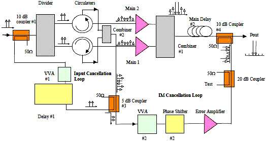
Figure 1b - Parallel Combined RFAL Amplifier (PC-RFAL) using
circulators.
Signal Sampler:
The input signal splits even by using an in-phase divider. Directional
10 dB couplers #1 and #2 samples both the forward and reflected signal at the input
of the Main amplifiers. Circulators can replace the 10 dB couplers and provides
better performance but at a higher cost and size as shown in Fig 1b.
The reflected signal from the main amplifiers contains the suppressed level of
the fundamental carriers, the level depending on how well the input of the transistor
is matched to the source. (Normally >15 dB of return loss). When the operating
input level drives the transistor into the non-linear range, the transistor produces
output distortion products that also appear at the input together with the reflected
fundamental carrier signals. This composite signal is used for forming the proper
error cancellation signal to be coupled to the output of the combined amplifier.
Ideally the error signal that cancels all the distortion at the output of the
combined main amplifiers should contain only the distortion products and zero fundamental
input carrier signals. The circuit "Input Signal Cancellation Loop" is used for
significant input carrier cancellation its main purpose is to reduce the overall
average power handled by the error amplifier over its operating frequency and amplitude
range.
The reflected signals of both amplifiers are combined and fed to a summing coupler.
The value of the coupler should be as high as possible for minimum insertion loss
in the reflected path containing the desired intermods that are used to develop
the error signal. The coupled signal must provide sufficient input signal at the
sum port to cause maximum cancellation of the input fundamental components to the
input of the error amplifier over the operating bandwidth.
Input Signal Cancellation Loop
The forward port of the Main 1 amplifier's 10 dB directional coupler #2 samples
the input signals. The coupled fundamental input signal is attenuated by a VVA #1
and is properly phased through #1 a variable and fixed delay and fed to the summing
coupler port #3. (The VVA and Delay could be replaced with an I/Q vector modulator).
If there is not sufficient input signal used for deep fundamental cancellation an
in-phase coupler can be used to sum the forward signal from both main amplifiers.
For the circulator configuration a 10 dB coupler is used at the input of the divider
to sample the incoming signal.
IM Cancellation Loop.
The composite error signal at the output of the summing coupler #3 is linearly
amplified and phased to the correct level and fed to the summing port of the 10
dB coupler #4 connected to the main delay line. The final composite error signal
mixes with the distortion products of the combined main amplifiers and causes significant
cancellation of the IM distortion.
The delay #1 and VVA #1 and VVA #2 elements are best adjusted with an input (peaked
phased) multitone signal spaced so that at least two thirds of the operating frequency
spectrum range at the max expected nominal operating power of the PC-RFAL. This
will provide the most optimum linear operation versus frequency and output power
range. (The variable portion of the delay and VVA can be replaced with an IQ Vector
Modulator to save space.)
The error amplifier has to overcome the losses of the reflected signal traveling
through the couplers, divider VVA, delay etc. (The circulator configuration has
lower losses than the couplers and requires a lower gain amplifier). The error amplifier
must amplify the error cancellation signal to the proper level at the summing coupler
#4 without adding any new distortion. The error amplifier should have a 1 dB CP
of 10 dB higher than the maximum signal handled through the IM cancellation loop.
An input bandpass filter may be necessary to prevent error amplifier overload.
Main Delay Line
The output signal and the error cancellation signals must have the same time
of arrival with opposite phase at the output of the coupler to cancel the intermodulation
distortion. The IM Cancellation Loop will have a longer delay than the Main Amplifier's
path. Use of a low loss delay line is recommended. Note that it is possible to operate
at multiple delay wavelengths from the optimum but this reduces the operating bandwidth
and increases losses.
Output Summing Coupler and Combiner
The Main Delay Line connects to the 10 dB output directional coupler #4, a 10
dB coupler is a good trade-off for low output signal insertion loss and reasonable
IM Loop loss. The forward port is terminated in 50 ohms. This load must be capable
of dissipating the coupled output signal plus most of the error signal. The summing
port is used to feed the error signal that cancels the distortion products from
the main amplifiers.
The delta IM cancellation improvement ranges from 10 to 30 dB for the IM3 Loop
ON/Off; IM5 cancellation delta improvement of around 5 to 20 dB for the IM5 Loop
ON/ Off; IM7 cancellation around from 5 to 15 dB for the IM7 Loop ON/OFF over the
whole frequency and power level range.
Prototype Performance.
The prototype PC-RFAL was designed to operate at an average power of +28 dBm,
875 MHz center frequency with a 20 MHz operating bandwidth. This band was selected
only because of equipment and parts availability. See the detailed circuit of the
basic main amplifier schematic in Figure 2.
The individual Main amplifiers use a single GaAs FET type Mitsubishi MGF2445A
biased at Vdrain = 9 volts
Idrain = 350 ma with a 1 dB gain compression of +28 dBm. The circuit contains
a LM337 variable DC regulator to maintain the FET drain fixed at 9 volt and has
a protection shut down circuit in case of failure of the negative gate voltage supply.
Note: Minor individual adjustment of the gate bias point of each main transistor
was used to best match their individual performance.
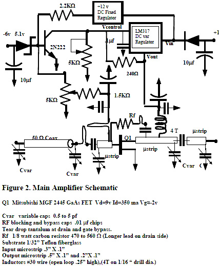
Figure 2 - Main Amplifier Schematic
| Freq 800 to 960 MHz |
|
|
| Gain= 16 dB |
Flatness= +/- 0.25 dB |
|
| RLinput= -20 dB |
RL out= -12 dB |
|
| P1dB CP=28 dBm |
IP3 =40 dBm |
(Two tone 875 and 876 MHz @ Pout +21 dBm ea tone) |
| Vdrain= 9v |
Idrain= 350 ma |
Vgate@ -2 volts |
The Error Amplifier used has a flat gain of over 50 dB with a 1 dB compression
point of +28 dBm and IP3 of 42 dBm. It uses +15v at 750 ma. This amplifier was selected
to make sure it had sufficient linearity over the full range of the Main Amplifiers
and not interfere with their performance. The PC-RFAL amplifier operates at +28
dBm or 4 dB back-off from the 1 dB CP of +32 dBm. At the +28 dBm level for the PC-RFAL
the error amplifier has to handle a +8 dBm composite signal. A more efficient error
amplifier with a lower gain and a +20 dBm 1 dB CP could replace the one used.

Figure 3 - Gain & Fundamental Reflected Signal Cancellation.
The 850 to 900 MHz swept frequency performance of the combined PC-RFAL is shown
in Figure 3 at an input of +10 dBm. (Trace 1). The PC-RFAL provides a nominal 15
dB gain with minor change from IM Loop ON or OFF condition. (See Trace 2a for IM
Loop OFF and Trace 2b for IM Loop ON)
Note that the PC-RFAL circuit's operational bandwidth is listed from 865 to 885
MHz frequency range but it can provide significant linearization over a greater
operational bandwidth. Better performance was achieved with the circulator configuration
resulting in a 30 MHz operational BW, a little better IM cancellation, slightly
higher power and with lower error amplifier gain.
The IM Loop ON condition maintains the amplifier's gain linear up to +2.5 dB
above the typical 1 dB compression point of IM Loop OFF condition. The tradeoff
when operating above or near the compression point is that it requires a larger
error amplifier that is able to handle the increasing amplitude of the error signal.
Operation of output power up to the 3 dB back-off from 1 dB CP (@ IM Loop OFF) allows
use of a lower level amplifier that improves the overall efficiency of the PC-RFAL.
Trace 3 in the plot represents the fundamental signal power in dBm versus frequency
of the reflected input signal at the 20 dB test coupler located at the output of
the error amplifier. As previously discussed the lower fundamental level reduces
the maximum power that the error amplifiers must handle over the operating frequency
range and improves the overall efficiency of the PC-RFAL. A deep fundamental cancellation
depends on the flatness and phasing of the Main Amplifier's reflected input signal.
Better Main input matching or a shaping network could be used to broaden the cancellation
over a wider frequency range.
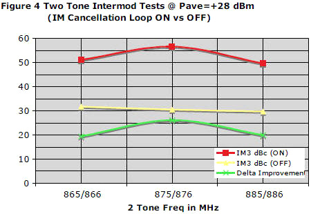
Figure 4 - Two Tone Intermod Tests
@ Pave=+28 dBm (IM Cancellation Loop ON vs. OFF)
The PC-RFAL intermodulation products were measured at set frequencies with two tones
spaced 1 MHz apart. Set frequencies of (865, 866 MHz), (875, 876 MHz), and (885,
886 MHz), with a per tone output power level of +25 dBm. The error amplifier's DC
power was turned ON and OFF and the peak delta from carrier to the IM3 products
in dBc was measured and plotted. An ON/OFF delta improvement of equal or greater
than 20 dB is shown in the graph. A better than 30 dB delta improvement is possible
if the circuit is tuned for a narrower frequency band or at a lower output power
level range.

Figure 5 - Output Power, Error Amplifier Power and Intermod
Delta Improvement vs. Two Tone Input Power.
The PC-RFAL's input was driven with two-tone signals at 875 and 876 MHz from
+11 to about +18 dBm average. The IM3, IM5 and IM7 intermods were measured referenced
to the carrier tones and the peak dBc measured with the error amplifier ON and OFF.
The two measurement were subtracted for each intermods and plotted. The IM3 delta
shown is over 25 dBc for most of the input/output range. As the output power gets
close to the 1 dB compression point the delta improvement tapers off fast. At this
point the error amplifier is at its limit in linear operation and degrades the PC-RFAL
performance.
Output Spectrum with 8 Tones. Performance set at average composite Pout of +22
dBm.
(8 Carriers Peaked Phase with Spectrum Analyzer on peak hold and 2 MHz carrier
separation)
Center tone is missing to measure the worst case intermod.
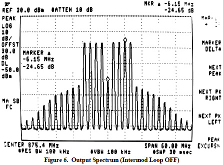
Figure 6 - Output Spectrum with Intermod Cancellation
Loop OFF Worst case IM= 24.65 dBc
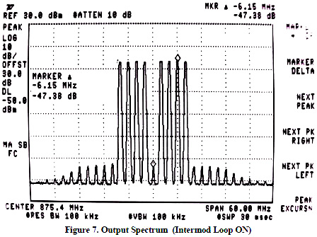
Figure 7 - Output Spectrum with Intermod Cancellation
Loop ON Worst case IM= 47.38 dBc
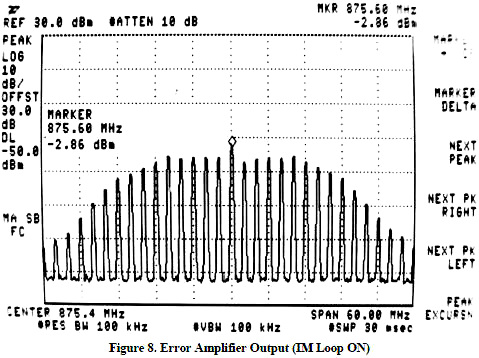
Figure 8 - Error Signal Output Spectrum with 8 Tones. Performance
at PC-RFAL average composite Pout of +22 dBm. (8 Carriers Peaked Phase with Spectrum
Analyzer on peak hold and 2 MHz carrier separation.)
Conclusion:
The work shows two new configurations of the basic Reflect Forward linearization
technique that has some efficiency advantages over previous methods. An important
feature of the RFAL configuration is that with the cancellation Loop in the OFF
condition the amplifier has the same basic performance of a non-linearized amplifier.
(Except for small delay, coupler and/or circulator losses). This allows the
possibility of a simple circuit to shut-down the IM cancellation loop when the input
signal level is low and the amplifier has acceptable IM performance. This will further
improve overall amplifier efficiency and makes it possible to use these configurations
from low noise to high power levels.
The present configuration can be arranged in a circular shape for an "n" number
of amplifiers connected to radial combiners and dividers and mounted to a cylindrical
casing to dissipate the heat. By using lower power, cheaper, transistors to reach
the desired power and linearity levels it is easier to thermal manage the design,
reduce size and make it more economical.
The US Patent 6,573,793 has not been renewed therefore all the circuits are available
for free commercial use. Hopefully someone will find them useful and put them to
work in a real product. This work was mostly done in 2008 and finally I found the
time to write it up and publish it before is totally forgotten. Most likely will
be my last.
Reflect Forward Linearizer for Combined Amplifiers, by Ray Gutierrez
(click for PDF file)
Posted 2/28/2012
|