|
April 6, 1964 Electronics
") [Table of Contents] [Table of Contents]
Wax nostalgic about and learn from the history of early electronics.
See articles from Electronics,
published 1930 - 1988. All copyrights hereby acknowledged.
|
Whilst reading articles on semiconductor
research and development in the era of this 1964 Electronics magazine,
it often occurs to me that much of the terminology presented is new to most people
in the electronics field, having been just recently coined by those developing the
technology. To wit, here author Landress shows diagrams of planar and mesa structures
for transistors. We are so familiar by now with those configurations that it hardly
seems there was a time when engineers did not speak so matter-of-factly of them.
Hole and electron mobilities were terms familiar to a niche group of atomic materials
scientists a decade earlier, as were diffusion depth and doping concentrations.
As the 1919 electronics practitioner would confabulate upon matters of
thermionic
emission and getter flashing in vacuum tubes, so, too, in 2019 do our kindred speak with
familiarity of electromigration and
minority carriers semiconductors.
New Technology Sparks an Expansion for Germanium Transistors

The Author
K.B. Landress is a senior project engineer in the Semiconductor Research and
Development Laboratories; responsible for design of planar germanium very-high-frequency
amplifier transistors and management of the germanium passivation development project.
He was a member of the International Operations Department from 1958 to 1961.
Before coming to TI, Landress was employed as an engineer by the firm of A. Earl
Cullum, Jr., Consulting Radio Engineers.
General-purpose germanium transistors can now be built with a planar structure,
possibly extending applications to phased array radar, tv tuners and computer switching
circuits.
By K.B. Landress
Senior project engineer, Semiconductor-Components Division, Texas Instruments
Incorporated, Dallas, Texas.
Although the first commercial semiconductor devices were made of germanium 15
years ago, silicon devices have outstripped them in the high quality device area,
even though germanium has better high-frequency electrical characteristics. The
reason is simple: Silicon transistors are easier to build to the tighter dimensions
required for devices that operate at high frequency. In fact, commercially it has
been impossible to build germanium transistors with good high-frequency characteristics
beyond 5 gigacycles.
That's why the heterogeneous oxide technology developed at Texas Instruments
Inc. looms so significantly. With it, the circuit designer can have general-purpose
germanium transistors with excellent high-frequency characteristics at costs that
compare favorably with present germanium mesa structures. The company can build
germanium transistors to almost any dimensional tolerances. This development may
mean an expansion for germanium as a semiconductor material even in such applications
as L-band phased array radar, television tuners and computer switching circuits.
The single most significant feature of the germanium planar transistor - in itself
a major development - is its structure. Now for the first time it is possible to
manufacture the very small device structures required for outstanding performance
in the 1 gigacycle to 5 gigacycle range.
In the past, the design engineer has been severely limited in the size of the
active areas of the transistor because of the exponentially increasing difficulties
of assembling smaller and smaller structures. This limitation has been overcome
by the use of expanded contacts, which are described later.
The outstanding electrical performance in the 1 Gc to 5 Gc frequency range will
be provided primarily through increased values of the maximum frequency of oscillation,
much lower values of extrinsic base resistance, lower noise figure, significantly
lower values of capacitance between the three terminals of the device, and improved
gain-bandwidth product. In addition, higher production rates than with mesa transistors
are achievable because the lead attachment problem has been lessened.
Planar Technology
Development of the planar technology for silicon gave a boost to the use of silicon
transistors because the planar process provides inherent surface passivation and
also allows using photographic masking in the manufacturing process. Latter is particularly
important for high-frequency transistors because photographic masks give higher
resolution than metal masks and therefore allow making small, closely controlled
junction areas. This small size and close spacing between collector and emitter
results in lower junction capacitance and smaller base resistance than in mesa transistors
with resulting higher frequency operation and lower noise figures.

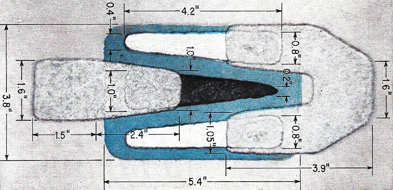
Planar germanium transistor has alloyed p-type emitter stripe
and two alloyed base stripes.
The present standard technology for germanium has been limited to the mesa type
of device shown in the illustration. A key reason for the interest in germanium
is that it has higher hole and electron mobilities than silicon, and is therefore
inherently capable of operating at higher frequency. Germanium also lends itself
to automation more readily than does silicon.
Thus, a germanium planar transistor should be useful wherever high frequency
(1 to 10 Gc) transistors are desired at operating temperatures below 100°C.
This would include consumer electronics and computer switching, for example.
Fabrication of silicon planar transistors involves growing a passivating layer
of silicon monoxide thermally on the surface of the silicon substrate and then etching
through this oxide layer. This technique cannot be used with germanium because germanium
monoxide has a high vapor pressure and would simply evaporate. However, a technology
has been developed that combines the inherent high-frequency capabilities of the
germanium mesa structure with the high mechanical resolution techniques used in
manufacturing silicon planar transistors. This technology shows promise of providing
devices with excellent high-frequency characteristics in the 5 to 10 Gc range, and
also devices with low noise figures in the 1 Gc to 3 Gc range.
Successful mating of the two technologies meant solving several basic problems.
One was to discover a material suitable for diffusion masking and insulating the
contacts. This was accomplished by a technique in which an amorphous film of silicon
dioxide is deposited at high temperatures on germanium. This method, which requires
careful control of impurities and of film deposition to avoid pinholes, can be used
to produce a planar collector-base junction with extremely sharp breakdown characteristics
at the knee of the reverse voltage-current curve. Typical reverse characteristics
are shown in the oscilloscope trace.
Glass Masks
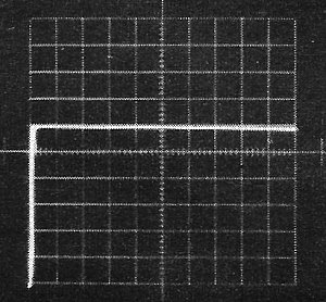
Reverse collector-base characteristics. Vertical scale is 5 v/div.
horizontal is 10 microamp/ div.
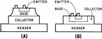
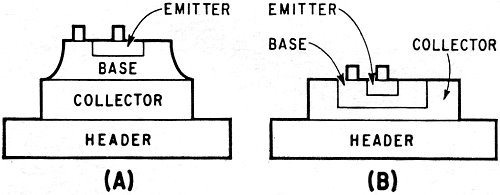
Basic structure of mesa transistor (A) and planar transistor
(B).
In the production of the typical germanium mesa transistor, the geometric patterns
of the alloyed emitter and the base contact are produced by vacuum evaporation of
the desired materials through metal masks. The definition of the resulting patterns
is naturally limited by the definition of the metal mask patterns. In addition,
the minimum linear-device dimension that can be obtained is controlled by that obtainable
in metal mask fabrication. The present state of the art in metal mask fabrication
limits the minimum linear dimension to approximately 0.0005 inch with a definition
permitting adjacent metal areas to be separated by 0.0005 inch. These values can
only be obtained if the geometric pattern is limited to a relatively simple shape.
By way of contrast, the glass photographic masks employed in production of silicon
planar structures are limited to a minimum linear dimension of approximately 0.0001
inch with a definition adequate to permit separation of distinct areas by 0.0001
inch.
Early in the development program, it was recognized that for the germanium planar
transistor to reach full potential, the use of metal evaporation masks would have
to be discontinued. Consequently, a technology based on glass photographic masks
was developed to provide formation of the geometric metalized device areas. The
decision to continue the alloyed emitter structure of the germanium mesa devices,
rather than pursue the diffused emitter structure of the silicon planar devices
was made because of the theoretical advantages of the alloyed emitter structure.
As a result of the development activities, well-defined metalized areas with a minimum
linear dimension of 0.0003 inch are being produced routinely. The processing steps
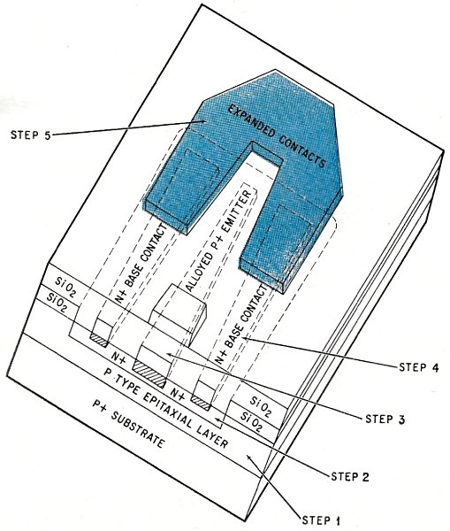
that were finally developed are outlined below.
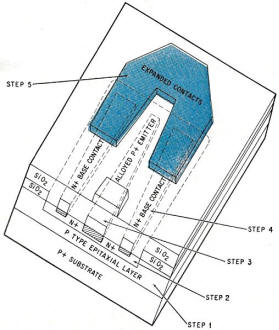
1) Slice preparation
The basic substrate material (see diagram) is obtained from a gallium-doped,
germanium, single-crystal of 0.002 ohm-centimeter resistivity, oriented in the 110
plane. The sliced crystal is chemically polished to provide a smooth surface. A
vapor deposited epitaxial layer of 1 ohm-centimeter resistivity is grown on the
lapped and polished substrate. The thickness of the slice is approximately 5 mils.
The completed epitaxial material is placed in a specially designed SiO2
reactor where a 2,000 angstrom SiO2 film is deposited onto the epitaxial
layer by the pyrolytic decomposition of tetroethoxysilane. Through the use of photolithographic
techniques, windows are etched out of the SiO2 film in preparation for
the base diffusion.
2) Base diffusion
The slice is then placed into a diffusion chamber at elevated temperatures and
arsenic is allowed to diffuse for a specified length of time into the epitaxial
layer through base windows etched out of the SiO2 film in step 1. Arsenic
is vaporized at an elevated temperature and is transported across the slice using
a constant flow of gas consisting of a mixture of hydrogen and nitrogen.
3) Emitter stripe deposition
A continuous film of Kodak metal etch resist (KMER) is placed on the entire surface
of the base-diffused side of the slice. With the use of a glass photomask, the emitter
stripe design is etched into the thin film of KMER. A continuous film of emitter
material is then vacuum deposited on top of the KMER film. A second KMER film in
the outline of the emitter, on registry with the original emitter windows, is placed
onto this film of emitter material. After etching away the exposed emitter material,
the "top-hat" KMER film is removed, leaving a well defined, desired emitter pattern.
The emitter stripe is alloyed at elevated temperatures.
4) Base stripe deposition
The ohmic-base contact is fabricated by the same techniques employed for fabricating
the emitter. Highly conductive materials such as gold and silver are used in conjunction
with the appropriate impurity to provide ohmic contact to the base. The base stripes
are then alloyed at elevated temperatures to insure ohmic contact to the base.
5) Fabrication of expanded contacts
A continuous film of SiO2 approximately 3,000 angstroms thick is deposited
onto the slice (this is the second pyrolitic deposition). KMER techniques are employed
to cut a window through the SiO2 film to the emitter and base alloyed
stripes.
A relatively thick, continuous film of aluminum is vacuum-deposited on top of
the SiO2 film. KMER patterns in the outline of the desired expanded contact
area are placed on the thin film. After the etching of exposed aluminum film and
removal of the KMER "top-hat", the expanded contact appears well defined and of
the desired shape. These expanded contacts provide large metalized areas for attaching
the lead wires, the size of the lead wires no longer being limited by the minimum
dimension of the emitter stripe.
The remaining device assembly steps are consistent with those normally used in
fabricating germanium mesa devices except that no etching or wet processing is employed.
Design
Structure of pnp germanium planar transistor.
The capability of fabricating very small active regions in a device with relatively
complex geometric shapes permits the design engineer to exploit more fully the capabilities
of the basic germanium semiconductor material. The most obvious approaches in improving
the electrical device characteristics by geometry are the reduction in emitter area
and the use of the interdigitated geometry. The theoretical advantages of even the
simple interdigitated geometric pattern of one emitter stripe and two base stripes
in comparison to the usual mesa pattern of one emitter stripe and one base stripe
has long been understood.
The difficulties associated with providing lead attachment to three rather than
two distinct areas, however. have relegated this structure to small quantity, high
cost experimental laboratory devices. The use of expanded contacts to parallel the
individual areas while providing a large region for lead attachment should result
in the use of the interdigitated structure in future production device designs.
Prototype Unit
A prototype pnp germanium planar epitaxial transistor was designed to demonstrate
the capabilities of this type of structure and to evaluate further its production
aspects. The designed active areas of the germanium planar device were selected
to approximate those of the small germanium mesa device in high volume production.
A photograph of the geometric structure is shown on above. As seen, the geometric
design is an interdigitated structure of comparatively complex active device areas
paralleled by means of expanded contacts.
This prototype germanium planar epitaxial transistor was announced by Texas Instruments
Inc. at the IEEE meeting in New York last month. The transistor is designated as
the TI X-3032 and characterized as a general purpose 1 Gc amplifier/oscillator.
The typical high-frequency device parameters obtained in the laboratory are in the
table.
The TI X-3032 was not specifically designed to meet the requirements of any particular
application. To repeat, the purpose of design was to demonstrate the capabilities
and applicability of the basic structure to the 100 Mc to 10 Gc frequency range.
It is quite possible, however, that the specific design will find general acceptance
in several areas of application. It is considered a general-purpose transistor that
can be used in the same circuits as the germanium mesa transistor.
Electronics I April 6, 1964
Transistor Characteristics
f† - 750 Mc
fmax - 3,000 Mc
rb1 - 15 ohms
rb1Cc - 3.0 p sec
CTc 3.0 pF
Noise Fig. 2.5db @ 200 Mc
Sufficient time has not elapsed to permit any extensive high temperature storage
or operating life test data to be accumulated. Early indications are, however, that
the reliability is consistent with that expected from silicon dioxide surface passivated
structures. The mechanical reliability and the moisture resistance of the planar
structure have been proven superior to the mesa structure as had been anticipated.
No concrete statement of the device failure rate can be made until sufficient data
on all reliability tests is available, however.
The mechanical structure of the device should be greatly enhanced because the
expanded contacts permit using large diameter wires for leads. Moisture resistance
data shows that the planar structure is exceptionally superior to the ordinary mesa
structure where no surface protection is used, such as the silicon dioxide on the
planar structure.
Reverse leakage currents are comparable to those found in germanium mesa transistors.
Well constructed and carefully assembled mesa devices have reverse leakage currents
equal to the theoretical minimum obtainable for a given device area and material
resistivity.
The typical mesa structure, however carefully constructed, normally exhibits
a certain degree of rounding at the breakdown voltage knee. It has been established
that this rounding is caused by surface effects of the unprotected mesa structure.
The planar structure, because of its surface passivation from the silicon dioxide
film, exhibits extremely sharp breakdown characteristics at the knee (see oscillogram).
The breakdown voltages of the planar structure equal or exceed those obtained by
the mesa structure for equal values of starting resistivity and the same primary
diffusion.
Front Cover
Art director Howard Berry has symbolized the germanium planar transistor inserting
a representation of the structure into a giant TO-18 can. His representation shows
the alloyed p-type emitter stripe and two alloyed-base stripes. The violet area
is for the expanded contacts.
Posted March 15, 2019
|


")