|
January 17, 1964 Electronics
") [Table of Contents] [Table of Contents]
Wax nostalgic about and learn from the history of early electronics.
See articles from Electronics,
published 1930 - 1988. All copyrights hereby acknowledged.
|
According to author Albert
Hilbinger, good dynamic range down to DC and circuit simplicity offset the low efficiency
of Hall-effect modulators. The mixer circuit output has a suppressed carrier signal,
making it a true product of the two inputs (fLO ± IF in the frequency
domain). Evidently the scheme never gained wide acceptance in the industry because
a search of the term does not produce much - other than this article. Achieving
a suppressed carrier with standard diode mixers requires a quadrature arrangement
using two mixers and a pair of 90° power splitters, which nowadays is done handily
within a single integrated circuit. Sensors are the main exploitation for the
Hall
effect these days. They are widely used as proximity sensors, speed sensors,
position sensing, and current sensing.
New Uses for Hall-Effect Modulators
Hall modulators are inherently compact. Trimmer resistors of
Fig. 2B are seen in right view
By Albert R. Hilbinger
Aircraft Armaments Inc., Cockeysville, Maryland
Dynamic range down to d-c and circuit simplicity offset the low efficiency of
Hall-effect modulators. Output is a suppressed carrier signal, a true product of
the two inputs
Hall Efficiency
The main trouble with Hall-effect multipliers at present is their low efficiency.
Whether or not this efficiency can ever be substantially raised is problematical,
since it depends on a materials constant called the Hall coefficient. The Hall coefficient
is much higher for semiconductors than it is for metals but still leaves much to
be desired. But efficiency is only one parameter, and Hall multipliers have some
important advantages.
Hall effect devices are useful as modulators since their output voltage is proportional
to the product of two input voltages or currents.1, 2, 3, 4 In spite
of an inherently low efficiency, Hall-effect multipliers offer the advantages of
simplicity and wide dynamic range.
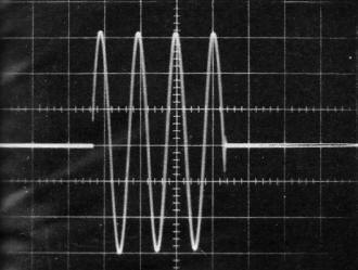
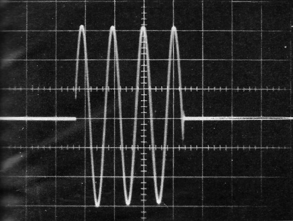
Waveform of pulse-modulator output for 5-kc output.
Waveform of pulse-modulator output for 5-kc output (expanded)
Circuit - Hall output voltage, as indicated in Fig. 1A,
is
Eh = (RhIcB/t) X 10-8 volt (1)
where Rh = Hall coefficient (a semiconductor material constant) in
cm3/coulomb, Ic = semiconductor element control current in
amperes, B = magnetic flux density in gauss, and t = semiconductor element thickness
in centimeters.
Flux density produced in an air gap in a ferromagnetic core operated below saturation
can be expressed as
B ≈ 0.4πNIb/Lg
(2)
where N = number of turns in coil wound on core, Ib = coil current
in amperes, and Lg = length of air gap in core in centimeters.
Substituting Eq. 2 for B in Eq. 1 and combining constants yields
Eh = KIcIb (3)
where K = 0.4 πNRh X 10-8/t
Lg
Thus the Hall voltage is a true product of two applied currents. If the currents
are expressed in terms of the voltages which produced them
Eh = K'EcEb (4)
where K' = K/Rc Rb; and Rc = resistance of control-current
input circuit and Rb = resistance of field-current input circuit.
Modulation - If the two inputs are sinusoids Ec = Eoc cos
ωct and Eb = Eob
cos ωct, the resulting output product
is
Eh/K' = EcEb = EocEob
cos ωct cos ωbt (5)
Letting Eoc Eob = Eo and applying the appropriate
trigonometric identity
Eh/K' = (Eo/2)[cos (ωc
+ ωb)t + cos (ωc
- ωb)t]
(6)
If Ec is a carrier frequency and Eb a modulating signal,
Eq. 6 represents a modulated wave. The equation has two sideband terms, (ωc + ωb) and
(ωc - ωb)
and no carrier term (a term in ωc only). Thus the resulting output is
a suppressed carrier or balanced modulator signal; the Hall-effect multiplier is
inherently a balanced modulator.
Applications - A number of applications employing Hall-effect
modulators have been investigated and three will be described. In all cases the
same basic physical construction was used. A rectangular indium arsenide (InAs)
element is cemented to a ferrite disk and then lapped to the desired thickness.
Four electrical connections are made to the semiconductor element as shown in Fig. 1
B. The ferrite disk-semiconductor element assembly then becomes an integral part
of the magnetic structure, as shown in Fig. 1C. The magnetic field through
the semiconductor element is produced by a current flowing in a coil wound on a
bobbin which is mounted around the center ferrite post of the assembly.
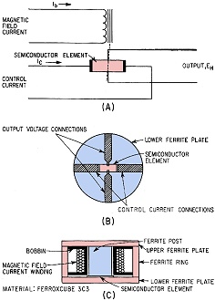
Fig. 1 - Output of Hall-effect device (A) is a voltage proportional
to the product of control current and magnetic flux. Electrical connections to semiconductor
block (B) and cross section of multiplier (C). The magnetic circuit is operated
in its linear region to keep saturation nonlinearities from affecting the output.
In one application a carrier frequency of approximately 1-Mc is modulated with
a fixed frequency of 400 cps. Theoretically, either signal could be applied to either
input. The practical choice, however, is to use the carrier frequency as the control
current and the 400 cps as the magnetic-circuit drive, as shown in Fig. 2A.
Core losses in the ferrite material used would be high at 1-Mc whereas the semiconductor
element is essentially a pure resistance. The magnetic field coil is then series
resonated to minimize the input power. Output is applied to a load of approximately
15 pf. Since input frequencies are fixed, it is possible to resonate the capacitance
with a high-Q inductance that is link-coupled to the output of the Hall-effect multiplier.
With no modulating voltage applied, but with maximum carrier input, the output
voltage is nulled with R1. This minimizes the in-phase component of what
is generally called the zero-field voltage. This voltage also contains a quadrature
component that is eliminated by adjusting C1. After potentiometer R1
is adjusted, maximum modulating signal amplitude is applied and C1 is
adjusted for zero output at the points of modulation envelope cross-over.
In many Hall-effect modulator applications the leakage component inductively
coupled from the magnetic field to the output must be removed. In this application
this component was eliminated by the narrow-band output circuit.
Modulator output voltage is linear within one percent of full scale from zero
to peak-field excitation of ±12 ampere-turns. With 850 milliwatts of carrier
power and peak-field excitation of 12 ampere-turns, a modulated 100 volts peak-to-peak
was obtained. The output could be increased by using a multiplier ferrite core material
with a higher saturation flux density or by using a higher Q output transformer.
A 50-percent increase in output level could be achieved with presently available
optimum core materials for both multiplier and output transformer, with no increase
in input power.
Pulse Circuit - In a second application a Hall-effect multiplier
was used to produce bursts of audio-frequency signals, is indicated in Fig. 2B.
Audio response of the unit is from d-c and is down 3db at 20 kc; there is no low-frequency
cutoff. Pulse input requirements are one ampere peak at a maximum duty cycle of
0.1. For lower duty cycles peak current can be increased, with the restriction that
the average pulse power dissipated in the semiconductor element does not exceed
2 watts. Resistor R1 provides the audio bandwidth and matches the audio
input to a particular voltage source. Resistor R2 matches the pulse input
to a 50-ohm pulse source. Potentiometer R3 is adjusted for minimum pulse
output with no audio applied; potentiometer R4 is adjusted for minimum
audio output between pulses. For both R3 and R4, infinite
resolution trimming potentiometers are used.
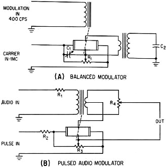
Fig. 2 - Balanced-Modulator circuit (A) with low frequency
applied to the inductive magnetic circuit and high frequency applied to the resistive
semiconductor. Pulse-driven circuit (B) can produce pulses of audio or an audio
signal sampled at a high pulse rate.
Results obtained with one-ampere peak pulses and 10 volts rms audio input include
an output of 350 mv peak-to-peak, with the output more than 65 db down between pulses.
The audio input could be increased to 100 volts rms without distortion, giving
an output of 3.5 volts peak-to-peak. But the audio rejection between pulses would
be degraded by approximately 20 db. Also, the peak pulse current could be increased
in accordance with the power restrictions mentioned. Operation at greater pulse
amplitudes with the audio input voltage held constant would improve audio rejection
between pulses. For maximum audio rejection under any conditions, the pulse source
should not have a d-c output level between pulses.
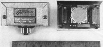
Oscilloscope photographs of the output waveforms of the modulator are shown and
also the unit packaged as a plug-in module.
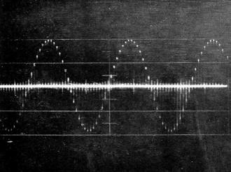
In a variation of the device, a pulse repetition rate higher than the audio frequency
was used. Output characteristics are similar to those of the preceding modulator.
If a number of pulses per cycle of audio are desired, the audio range is restricted
by the pulse requirements. For example, at one ampere peak pulse current, if the
pulse width is 10 microseconds and the duty cycle is 0.1, the maximum prf is 10
kilocycles. For ten pulses or more per cycle of audio under these conditions, the
maximum audio frequency is one kilocycle. By reducing the peak pulse amplitude,
a higher duty cycle could be employed, thereby allowing higher audio frequencies.
A possible application for this mode of operation is the detection of low-frequency
magnetic fields. The physical construction previously described could not be used;
instead, the magnetic field would be applied to the semiconductor element with flux
collectors or magnetic antennas.
Other modulator applications covering a wide range of frequencies have been described
in the literature.5, 6, 7 The potentially rugged simplicity, low cost,
and wide dynamic range of the Hall-effect modulator make it ideal for a wide range
of applications where a true-product, suppressed-carrier device is required.
References
(1)W. A. Scanga, A. R. Hilbinger, and C. M. Barrack, Hall Effect Multipliers,
Electronics, July 15, 1960, p 64.
(2) G. L. Keister, A Compact Multiplier Puts The Hall Effect to Work, Control
Engineering, Nov., 1955, P 94.
(3) R. P. Chasmar and E. Cohen, An Electrical Multiplier Utilizing The Hall Effect
in Indium Arsenide, Electrical Engineering, Nov., 1958, p 661.
(4) G. S. Glinski and T. P. Landolt, Theory and Practice of Hall Effect Multipliers,
1961 TRE International Convention Record, Part II.
(5) Armour Research Foundation of Illinois Inst. of Technology, "Instrumentation
and Measurement Techniques Study", Signal Corps Contract No. DA 36-039 SC-78269,
Quarterly Progress Report Nos. 2, 3, 4, 6, 7 and 8.
(6) E. Cohen, Hall Effect Multiplier for Use at Radio Frequencies, Electronic
Engineering, 32 p 558, 1960.
(7) E. Cohen, An Improved Radio Frequency Hall Effect Modulator, Electronic Engineering,
34 p 316, 1962.
Posted October 5, 2023
(updated from original
post on 9/25/2018)
|


")