|
May 1967 Electronics World
 Table
of Contents
Table
of Contents
Wax nostalgic about and learn from the history of early electronics. See articles
from
Electronics World, published May 1959
- December 1971. All copyrights hereby acknowledged.
|
If you are just entering the
field of electronics, the concepts presented in this half-century-old article for
basic field effect transistors (FET) are still relevant. Significant improvements have
been made since then, but the fundamentals stand. One of the most useful items in
this article is Table 1, which compares and contrasts vacuum tubes, bipolar junction
transistors, and field effect transistors. Topics covered include general properties
of FET's, source followers (a la emitter followers in BJTs), common source amplifiers
(a la common emitter amplifiers in BJTs), the Miller oscillator, combinations of
FET's and BJT's, and a gated amplitude modulator. See the original article
on FET's
in the November 1965 issue of Electronics World.
Field-Effect Transistor Circuits
By Joseph H. Wujek, Jr. and Max E. McGee
A grouping of six simple, low-cost circuits that illustrate many of the principles
of FET operation.
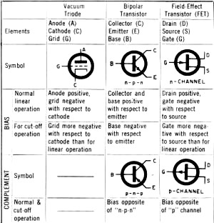
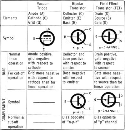
Fig. 1 - Tabular comparison of tubes, transistors, and FET's.
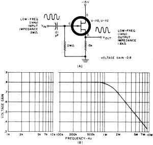
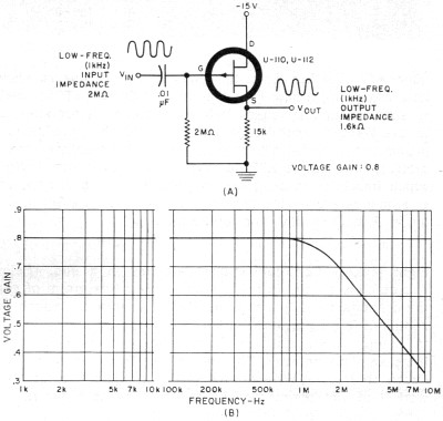
Fig. 2 - A source-follower circuit along with frequency response.
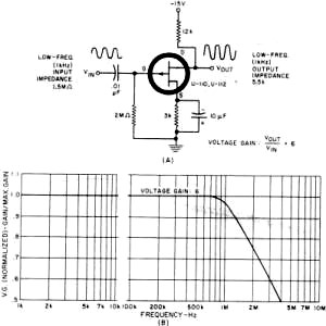
Fig. 3 - Common-source FET amplifier circuit along with response.
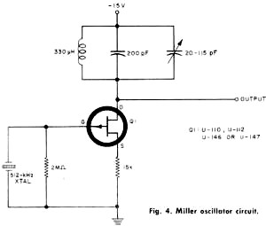
Fig. 4 - Miller oscillator circuit.
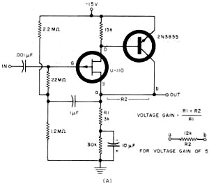
Fig. 5 - FET/Transistor pair has gain and high input impedance.
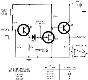
Fig. 6 - Pulse-stretcher circuit with FET and transistors.
One of the most important new semiconductor devices is the field-effect transistor
(FET). This article describes six low-cost circuits which may be built to demonstrate
the important properties of FET's. The U-110 and/or U-112 p-channel FET's are used
in the circuits discussed and are relatively low priced. Siliconix has offered the
U-110 and U-112 together as a package for $2.75. The U-110 may be had alone for
$1.00 under this offer. The industrial-type FET's, U-146 and U-147, are slightly
higher in price. The bipolar transistors used are General Electric epoxy devices
which sell for $0.50 to $1.00 each.
General Properties of FET'sFor convenience, the similarities
among vacuum tubes, transistors, and FET's are given in Fig. 1. We must recognize
the inherent differences which exist among vacuum tubes, transistors, and FET's
and the table serves only as an aid in pointing out bias polarities.
The FET resembles the vacuum tube in that the impedance looking into the gate
is very high and can be on the order of hundreds of megohms. Also, the FET is a
low-noise device, better than bipolar transistors and competitive with vacuum tubes.
On the other hand, FET's resemble transistors in the leakage currents which flow
between their electrodes when the device is cut-off.
The Source Follower
The source-follower circuit is analogous to the vacuum-tube cathode-follower
or transistor emitter-follower. We might expect similar behavior from these circuits
and such is the case. We thus have high input impedance, relatively low output impedance,
and a voltage gain that can be made very close to unity.
Fig. 2 shows a simple source-follower circuit and the bandpass characteristics
obtained with two different FET devices. The 2-megohm resistor establishes the gate
bias and is similar to the grid-leak resistor used in tube work. However, this resistor
must be made small enough so that increased leakage current between the gate and
source will not drastically change the bias. For the U-110 and the U-112, leakage
between gate and source at room temperature is on the order of 5 nanoamps (5 x 10⁻⁹
amp), so a 1or 2-megohm resistor is adequate.
At elevated temperatures the increase in leakage current would dictate that a
smaller resistor be used so as to reduce changes in bias with leakage current. It
is possible to bias FET's so that very small temperature drift results.
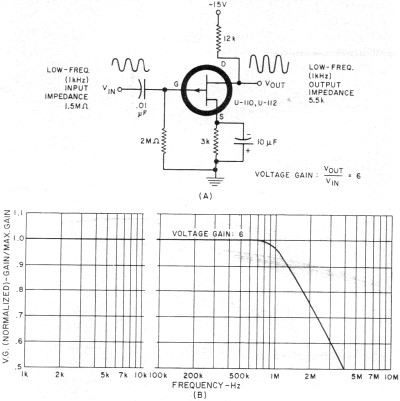
Common-Source Amplifier
The common-source circuit is analogous to the common-emitter transistor and common-cathode
vacuum-tube circuits. Again, properties of this circuit are similar to the transistor
and tube counterparts. Input and output impedances are intermediate in value and
a voltage gain greater than unity may be realized.
Fig. 3 shows a common-source circuit and the bandpass plot obtained by using
either the U-110 or U-112 FET.
Miller Oscillator
The very high input impedance of the FET enables us to build the simple Miller
oscillator of Fig. 4. The high impedance of the gate circuit results in light loading
of the crystal. The LC combination in the drain circuit is tuned to resonate slightly
below the parallel resonance of the crystal. For the type of devices considered
in this article, the upper limit of frequency operation is only a few megahertz.
For crystals other than the 512-kHz unit shown, the LC combination must be changed
accordingly.
The output of the oscillator will not tolerate much loading, but the source-follower
circuit can be used as a driver to provide low output impedance without loading
the oscillator stage excessively. With differences in FET types and layout details,
some modification of the LC network may also be required. For the circuit we tested,
"clean" oscillations were observed for the four FET types indicated on the figure
without retuning the circuit, and with the supply voltage varying from 6 to 22 volts.
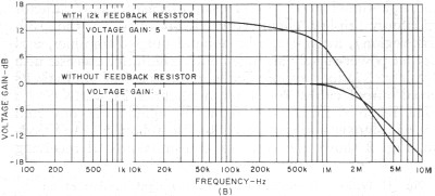
FET/Transistor Pair
A circuit which performs like an improved source-follower or emitter-follower
is shown in Fig. 5. The FET again provides very high input impedance, while the
transistor output provides low output impedance. Unlike the source-follower or emitter-follower,
this circuit can be built to have a voltage gain greater than unity. This is accomplished
by a resistor in the feedback path as shown in Fig. 5A (lower right).
Fig. 5B gives the bandpass characteristics when used with a voltage gain of unity
and with voltage gain greater than unity. The bandwidth is dependent upon the impedance
of the driving source. When driven by a 600-ohm test oscillator, the upper 3-dB
point is 2 MHz. Bandwidth decreases as the driving source impedance increases. At
low frequencies the amplifier input impedance is about 100 megohms and the output
impedance is less than 2000 ohms.
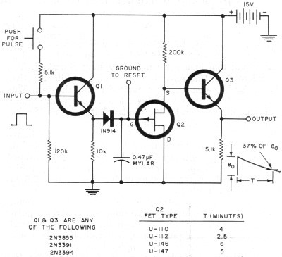
Fig. 6 shows a stretcher which senses the peak amplitude of a pulse and holds
this voltage level for a time much longer than the width of the pulse. The diagram
includes a push-button to provide the pulse, but of course the pulse could be coupled
in from a suitable external source.
Transistors Q1 and Q3 provide impedance transformation and isolate the FET from
both the source and the load. When the input pulse appears, the capacitor is charged
through Q1 and the diode. After the input pulse terminates, Q1 is cut-off and the
diode is back-biased. The input impedance of Q2 is very high so that the charge
leaks off the capacitor mainly by leakage current through the diode and the capacitor.
The FET (Q2) then presents the d.c. level to Q3 which acts as an output driver.
Fig. 6 also gives the duration of the output obtained with four different FET's.
(Note that the FET is connected in reverse in order to make the drain negative.)
The time constant can be increased by using an FET having a very low gate leakage
and by selecting a diode and a capacitor with very low leakage. By using these more
expensive components, FET stretcher circuits with output pulse times as long as
30 hours have been built. The circuit can be used as a peak-amplitude detector or
to obtain a required time delay. Reset is accomplished by either allowing the output
to decay or by shorting the capacitor to ground.
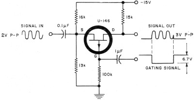
The FET can also be used as a linear gate or electronic switch as shown in Fig.
7. The resistance between source and drain with the switch "closed" is approximately
1/gm. With the switch "open", only a small leakage current flows between
source and drain. This type of circuit can also be used as an amplitude modulator.
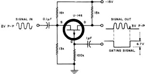
Fig. 7 - A linear gating or amplitude modulator circuit.
We have presented six simple, low-cost circuits that illustrate many of the principles
of FET operation. These circuits are designed to furnish an understanding of the
devices and to stimulate thinking toward other applications.
The authors wish to acknowledge the cooperation of Mr. Charles MacDonald
of Siliconix, Inc. and Mr. Al Kenrick of General Electric Company.
Posted July 22, 2019
(updated from original post on 3/1/2012)
|