|
September 1960 Electronics World
 Table of Contents
Wax nostalgic about and learn from the history of early electronics. See articles
from
Electronics World, published May 1959
- December 1971. All copyrights hereby acknowledged.
|
Transistors always have
been and always will be prone to damage or destruction if operated at temperatures
higher than their designed ranges. Modern foundry processes have made it possible
for greater heat tolerances for a given transistor size, but care must be taken
during circuit design to assure that the devices will under normal ambient conditions
not exceed their intended temperature range. Often a heatsink is required in order
to use a transistor at its full rated temperature, and sometimes extensive measures
are needed to keep the heatsink within an acceptable maximum temperature. Take a
look inside your computer for an example of how far heatsink technology has come.
The liquid-cooled
(desktop) and
heat pipe-cooled (laptop) schemes are amazingly efficient and capable of dissipating
heat from the CPU package, which would otherwise fry in milliseconds without it.
Don't Underrate Transistors
 By James R. Spencer By James R. Spencer
Explanation of maximum ratings of junction transistors and how to determine maximum
operating capabilities.
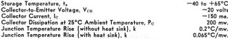
Table I - Absolute maximum ratings of typical junction transistor
used as example.
Normally transistors are not operated at their maximum ratings; however, there
are many times when it may be desirable to operate a transistor very close to these
maximum ratings. An understanding of the inter-relationship among the various maxima
is necessary if the demise of many a good transistor is to be prevented.
Manufacturers of transistors supply specification sheets which provide information
comparable to that found in a tube manual. Usually after a brief description of
the transistor and its mechanical specifications, the absolute maximum ratings are
listed. A typical list of such ratings for a germanium p-n-p junction transistor
is shown in Table 1. The transistor is a medium-power unit intended for audio-output
applications.
Storage Temperature
The storage temperatures are the two temperature extremes, low and high, to which
the entire transistor-case, leads, whiskers, and semiconductor blank - can be subjected
without permanent damage. The low-temperature extreme is usually determined by cold-induced
mechanical stresses which may cause the germanium blank to crack. The effects which
determine the high-temperature extreme are not as simple. For example, Ico,
the a.c. parameters, and the life expectancy of the transistor may all deteriorate
with extended storage at elevated temperatures. The results of transistor life tests,
however, indicate that life expectancy is an exponential function of the ambient
storage temperature and, therefore, the maximum storage temperature is usually chosen
to yield a reasonably high life expectancy.
The storage temperatures also have the following influence on transistor operation.
The transistor case temperature cannot be below the low-temperature extreme during
operation and the transistor junction cannot exceed the high extreme.
Maximum Ratings
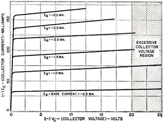
Fig. 1 - Collector curves showing limits due to voltage rating.
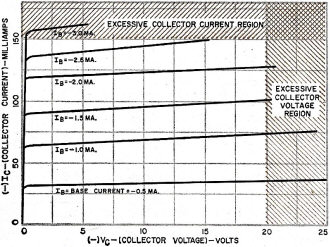
Fig. 2 - Limits imposed by collector voltage and current maxima.
The absolute maximum collector-to-emitter voltage is the maximum reverse voltage
which may be impressed between the emitter and collector without permanently damaging
the transistor. The value of this maximum voltage is usually determined by what
is known as punch-through. Punch-through occurs when the electric field generated
by the collector voltage extends completely across the base region. When this point
is reached, transistor action ceases and an extremely large current flows between
the emitter and collector.
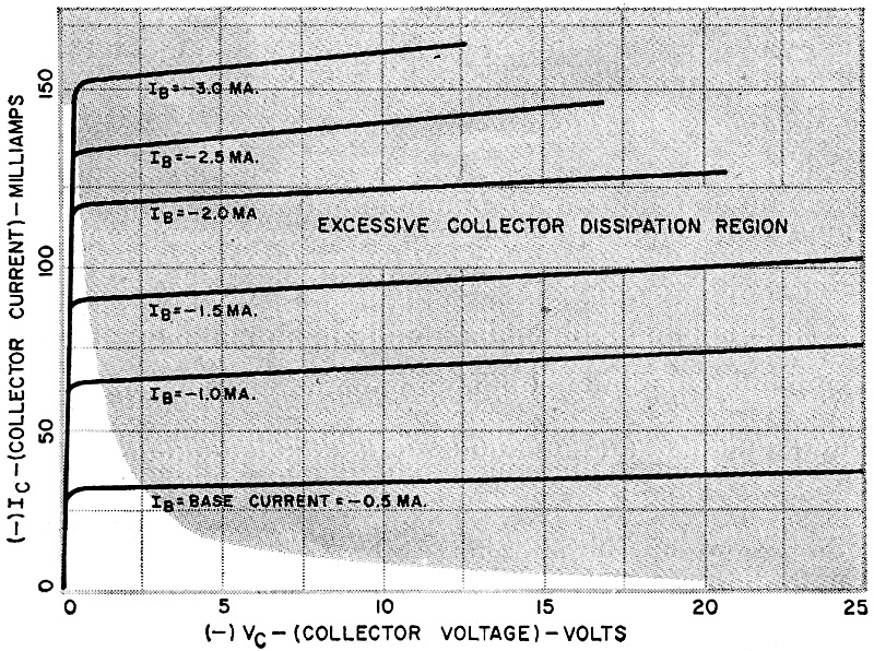
The common-emitter output characteristic curves for the transistor given in Table
1 are shown in Fig. 1. The diagonally hatched area indicates the region on the curves
where operation is not possible without exceeding the absolute maximum voltage rating
of the transistor.
The absolute maximum collector current is the maximum current which can flow
through the base-collector junction without irreversibly damaging the transistor.
This value is determined by the maximum current density the base-collector junction
can tolerate. It is a function of base-collector junction area, semiconductor material
resistivity, and is different for each type of semiconductor.
Fig. 2 shows the limitations placed on the output curves by both the absolute
maximum collector voltage and the absolute maximum collector current.
The product of the two maxima in Fig. 2 gives a power rating of 3 watts. The
manufacturer, however, has specified in Table 1 an absolute maximum collector dissipation
of 200 milliwatts at an ambient temperature of 25°C (77°F. See Table 2 for
converting centigrade to Fahrenheit.) The power dissipated within the transistor
and termed collector dissipation is the familiar I2R loss of electrical
power which is converted into heat. The maximum allowable collector dissipation
is a function of the thermal resistance of the junction and is limited by the maximum
allowable junction temperature. The maximum junction temperature is the same as
the high temperature limit of the storage temperature ratings discussed earlier.
The temperature of the junction is elevated above the ambient, or case, temperature
when the transistor is operating, due to collector dissipation. The junction temperature
may be calculated for any transistor using the equation: tj = ta
+ kPC ... (1)
where tj is the junction temperature, ta is the ambient
temperature, k is the thermal drop of the transistor, and PC is the collector
dissipation. Here k is a function of the mechanical de-sign and heat dissipating
mechanism of the transistor., Two values for k are given in Table 1; one for when
the transistor is used without a heat sink and the other for when an infinite heat
sink is used. The junction temperature of this transistor, when operated at the
absolute maximum collector dissipation specified by the manufacturer, can be obtained
by substituting values in equation (1) :
tj = 25 + 0.2 x 200
tj = 65°C
Collector Dissipation

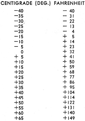
Table 2 - Temperature conversion table.
It can be seen from the above that the manufacturer has stipulated a maximum
collector dissipation rating that will provide safe junction temperature when the
transistor is operated at normal room temperatures. To illustrate the limitations
imposed by the maximum collector dissipation rating, a maximum power dissipation
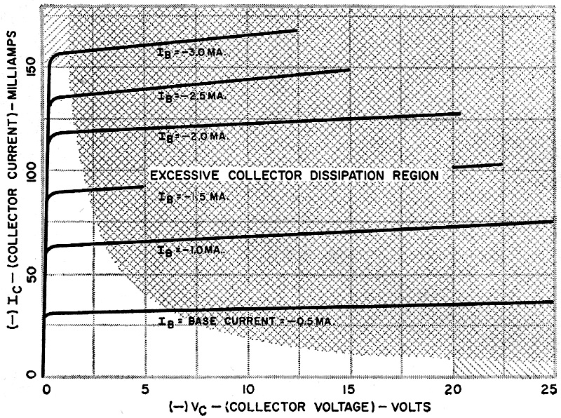
area is shown on the collector characteristic curves in Fig. 3. The cross-hatched
area indicates the region on the curves where operation at an ambient temperature
of 25°C is not possible without exceeding the absolute maximum collector dissipation
rating.
If the transistor is operated at an ambient temperature that is higher than 25°C,
the collector dissipation must be derated. For example, if the transistor is operated
in a sealed equipment case that also contains operating vacuum tubes, the ambient
temperature may be as high as 122°F. The maximum collector dissipation allowable
for operation without a heat sink at this ambient temperature can be determined
by a restatement of equation
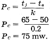
Thus it is possible to operate the transistor in an ambient temperature of 122°F
provided precautions are taken to limit the maximum collector dissipation to 75
milliwatts. The limitation imposed on transistor operation at 122°F ambient
is illustrated in Fig. 4. The relationship between collector dissipation and ambient
temperature shown in equation (2) indicates the possibility of safely operating
the transistor beyond the manufacturer's absolute maximum collector dissipation
rating if the ambient temperature is kept below 25°C.
One method of lowering the ambient temperature is to mount the transistor on
a suitable heat sink and then immerse the entire assembly in ice water to a point
just short of shorting out the transistor leads. Many mechanical arrangements can
be devised to obtain this type of ice bath, and with it, it is possible to maintain
an ambient temperature of 0°C (32°F).
The maximum allowable collector dissipation with a depressed ambient temperature
can be determined by substituting the appropriate values in equation (2).
PC = (65 - 0)/0.065
PC = 1000 mw.
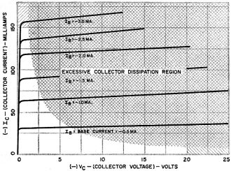
Fig. 3 - Limitation imposed by maximum collector dissipation
when transistor is operated at 25° C without using heat sink.
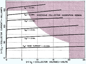
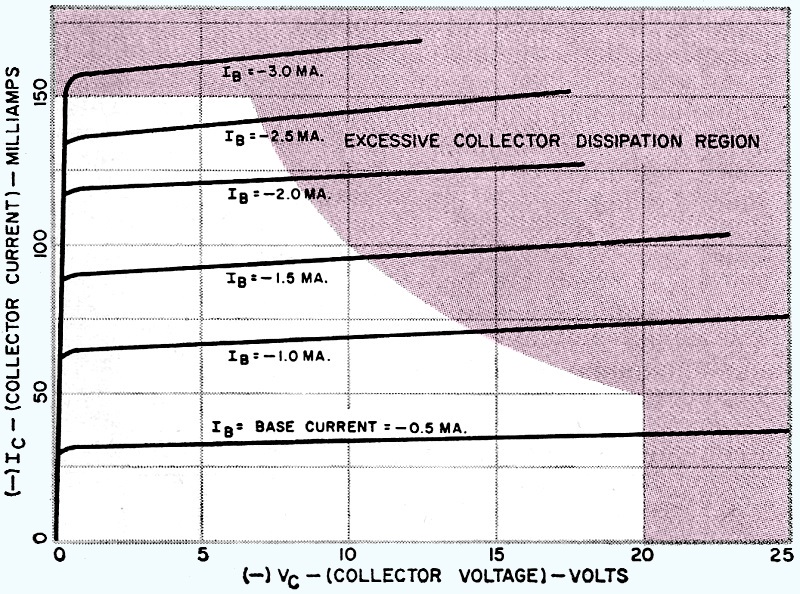
Fig. 5 - Collector dissipation limitations for operation at an
ambient temperature of 0° centigrade with a heat sink employed. Compare the
region of excessive collector dissipation shown here with that obtained under operating
conditions shown in the previous figure.
These calculations indicate that it is possible to operate the transistor with
a collector dissipation of 1 watt if the ambient temperature is 0°C. The new value
of k for operation with a heat sink was obtained from Table 1. Of course, for continuous
operation precautions must be taken to insure that the 0°C ambient temperature is
maintained Fig. 5 shows the output characteristic curves with the 1-watt power dissipation
curve. Since the power output of a transistor power amplifier is approximately equal
to collector dissipation times collector efficiency, any increase in collector dissipation
without exceeding the manufacturer's absolute maximum ratings results in increased
power output. Many manufacturers, rather than providing the values for k, give a
collector dissipation-ambient temperature derating curve. Fig. 6 is such a curve
for the transistor described in Table 1. From this curve it is possible to read
the allowable maximum collector dissipation in milliwatts for any ambient temperature.
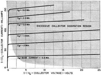
Fig. 4 - Limitation imposed by maximum collector dissipation
when transistor is operated at 50° C without using heat sink.
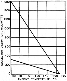
Fig. 6 - Collector dissipation versus ambient temperature derating
curve.
Posted August 27, 2021
|