|
June 1969 Electronics World
 Table of Contents
Wax nostalgic about and learn from the history of early electronics. See articles
from
Electronics World, published May 1959
- December 1971. All copyrights hereby acknowledged.
|
Crystalonics
is not a name that immediately comes to mind when thinking about semiconductor manufacturers. They appear
in this 1969 article in Electronics World magazine about power field effect transistors (FETs).
Many semiconductor companies came and went in the last days of vacuum tube active devices. Surprisingly,
a Google search revealed that Crystalonics
is alive and well in Ronkonkoma, New York. Per their website:
Formed in 1958, CRYSTALONICS is a broad line semiconductor manufacturer of
Small Signal Transistors,
JFETS,
Dual and Quad Transistors,
Power Transistors,
Current Regulator
Diodes, Varactor
Diodes and Custom Hybrid Microcircuits.
Most of the products are available in standard TO packages as well as
surface mount packaging
for Industrial, Military, and Space applications.
Well Shazam!, how have
I missed them lo these many years, especially since they make many
MIL-SPEC parts?
The Power FET
By John Tamosaitis
Applications Engineer, Crystalonics
A Teledyne Company
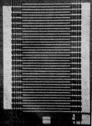
This large interdigitated chip by Crystalonics contains 40 individual channels.
Power field-effect transistors, capable of dissipating up to 8 watts, offer engineers new design
opportunities, but their operating characteristics need special care.
Engineers have been using field-effect transistors (FET's) for about eight years, but the majority
of such FET's have been small-signal devices rated at drain currents of 0.1 to 10 mA and drain voltages
of 5 to 30 volts. For the past few years, most new FET designs feature interdigitated structures, consisting
of a number of optimum-size channels connected in parallel. The optimum-size structure, having an average
drain current of 5 mA, is based on a compromise of characteristics and minimum resolvable dimensions.
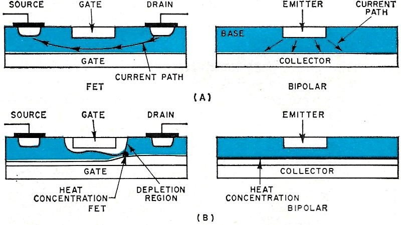
Fig. 1 shows a cross-section of an n-channel structure, similar to the one used in the power FET.
The bottom or "back" gate is uniform, while the top or "front" gate consists of a series of narrow diffused
strips. The isolation p-region surrounding the device is a deep diffusion which meets both the back
and front gates, thereby connecting them electrically. The device is actually made up of several channels
connected in parallel by a metallization pattern over a top oxide coating. Each channel has its own
source and drain contact; the contacts are in series (source-drain, source-drain), a front gate separating
each one. A front gate-isolation gate combination surrounds each contact.
Designing a channel in the bulk of the semiconductor overcomes the difficulty of a MOS structure,
which has its channel between a gate and a surface. Surface effects, such as ionization of absorbed
impurities, result in low output impedance and noise characteristics.
Theoretically, the channels can be stacked up indefinitely to produce FET's with drain currents of
up to 200 amperes, limited only by the size of the silicon slice. This is impossible in practice despite
the fact that the average number of defects per slice has plummeted over the years, resulting in generally
higher yields for all semiconductors. Field-effect transistors with drain current ratings of up to 1
ampere have thus become a reality.
Although several manufacturers presently supply FET's in the 100-mA range, they are specified and
packaged as low-power switching devices. Units like the 2N4091 in a heat-sink package handle up to 1
watt. Amelco and TI make a series of JFET's in the 10-mA range with drain ratings up to 250 volts, which
are also capable of dissipating 1 watt. Presently, the only true power FET is the CP650 series made
by Crystalonics. Packaged in a solid TO-5 can, they have an IDss as high as 1 ampere and
a maximum drain voltage of 25. These units closely resemble the interdigitated power transistor. Because
of their chip size and complexity (total channel length approximately 2 inches), the power FET is a
relatively low-yield, high-cost device.
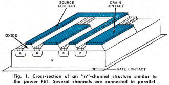
Fig. 1 - Cross-section of an "n"-channel structure similar to the power FET. Several
channels are connected in parallel.

Fig. 2 - Current paths in the FET and bipolar transistor (A). (B) Areas of heat concentration
are shown for comparison.

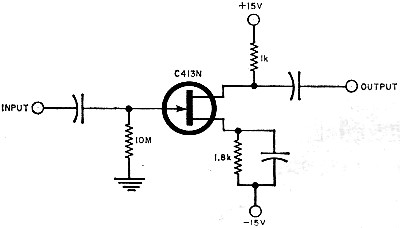
Fig. 3 - FET amplifier has a noise level of less than 1.2 μV.
Why a Power FET?
Power FET's enjoy several advantages over bipolar transistors:
1. They do not suffer from second breakdown, the hot-spot condition that lowers a bipolar's maximum
collector voltage as the current increases.
2. Having a negative temperature coefficient, thermal runaway is impossible in a power FET.
3. When maintained below breakdown voltage, power FET's are self-current-limited to IDss.
4. Because FET's have much higher power gain than bipolars, driver stages are unnecessary.
5. The FET does not saturate, permitting faster switching than that attained with bipolars.
While the power FET is technically superior to the bipolar and the SCR in many applications, its
higher cost ($42 in small quantities) places many of its uses in the luxury class. Where performance
is the overriding criterion, though, the power FET is often the only choice. With constantly improving
yields and higher volume, the power FET should, over the next few years, cut into the power bipolar
markets to the same extent that its small-signal cousin has in its sphere of application.
The Crystalonics device (lead photo) is a large (0.04 X 0.06 inch) interdigitated chip containing
40 individual channels, each 0.02 inch long. The top gate, which is only 0.0001-inch wide, adds all
the channels. The total channel is almost two in. long. The typical IDss value is 600 mA.
If a standard transistor had these dimensions, the peak collector current would be about 6 amperes -
10 times as great. It is rather easy to see why this large difference exists. Referring to Fig. 2A,
current in the FET flows from the drain between the gates to the source. In the bipolar, where the top
gate is equivalent to the emitter and the bottom gate the collector, the path is much shorter and less
restricted. Structurally, the power FET is equivalent to a 100-watt, 500-MHz bipolar power transistor.
As a rule of thumb, FET's need ten times the active area of bipolars for the same current-handling
capacity. Similar to the interdigitated bipolar, the power FET maintains its high-frequency performance
in spite of size because it is equivalent to a number of small-signal devices connected in parallel.
And, while the power gain of an FET does not increase with size, the junction capacity and small-signal
transconductance do. This means that the gain-bandwidth product remains constant and all impedances
are decreased proportionately.
Because the drain and source contacts are on the same side of the junction, the only breakdown path
is from the drain to gate. FET's feature a zener characteristic somewhat like a bipolar, exhibiting
avalanche breakdown instead of punch-through. Thus, no safe operating area is needed. Since the FET
is self-current-limited to IDss, there is no danger of transient current damage.
Most of the JFET parameters are more stable than those of the bipolar transistor because the JFET
parameters are purely bulk dependent. The negative temperature coefficient of IDss (approximately
-0.7%/mA) is contrasted to the reduction of input base-emitter voltage and increase of current gain
with temperature that causes thermal runaway in bipolars. Altogether, the power FET has fewer and simpler
failure modes than the bipolar; in fact, for reliability analysis, it is closer to a rectifier.
Both bipolars and FET's are limited to 200° C junction temperature, having similar thermal resistance
in the same package type. Although the FET has a slight advantage, owing to its larger chip size (see
Fig. 2B), this is balanced by the FET dissipating most of its power in narrow strips between the gates
on the drain side, rather than across the entire back junction, as in the bipolar.
The FET cut-off frequency, fT is determined by Gm and junction capacity. Because
the output capacity between drain and source is only in contacts and leads, it is less than 1 pF. Therefore,
the cut-off frequency is determined primarily by the feedback capacity between drain and gate, and the
Gm that drives it. The order of fT for the power FET is about 1 GHz.
At any frequency substantially below fT, the power FET has much greater power gain than
the bipolar. Even though it requires higher voltage drive, its input current is practically zero and
driver stages are not needed. It is interesting to note that bipolars have about 10 times the Gm
of an FET operating at the same current level, but FET's have a much higher effective beta - a sort
of backwards situation.
Because the FET is a majority-carrier device, it has two inherent properties which should be stressed.
One of the bipolar's principal noise sources is carrier recombination noise in the base. The FET is
free from such noise because the current flow mechanism is determined by majority carriers (electrons
in an n-channel), just as in a metal conductor. Also, in a bipolar, radiation reduces minority carrier
lifetimes and results in a degradation of the transport factor. This is not possible in a field-effect
device.
Field-effect transistors generate almost no odd harmonics, resulting in much lower cross-modulation
than that attainable with bipolars. For this reason, FET's are now used in most FM tuners for high adjacent-channel
rejection. For example, for a given two-input signal level where bipolars exhibit third-order products
about 60 dB down, the third-order products of small-signal FET's are about 110 dB down. Owing to its
high Gm, the power FET has a noise figure of under 3 dB at 30 MHz when driven from a 50-ohm
source. Small-signal levels do not have to be transformed to 1000 ohms to obtain a low noise figure;
and the FET is capable of handling an additional 30 dB of signal with the same intermodulation distortion
level. This 30-dB improvement is very significant where receivers must pick up weak signals in a high
signal-strength area, such as in a mobile receiver operating next to a kilowatt transmitter.
Because of their high power gain, amplifiers built with a power FET require fewer stages. Actually,
since the input impedance is so high, a complete amplifier can consist of an input transformer to raise
the signal voltage level and a single power FET.

Fig. 4 - An FET amplifier used as a CATV distribution amplifier.
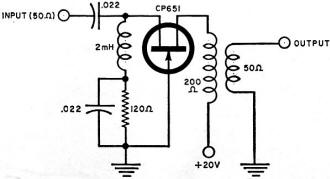
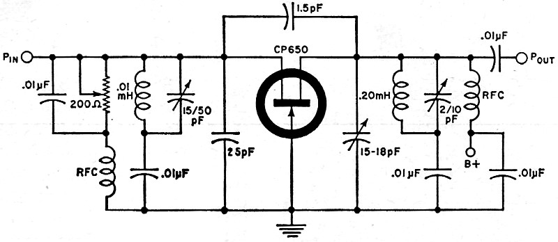
Fig. 5 - Broadband noise figure of this unit is less than 3 dB.
When run at low drain currents (approximately 10 mA), the power FET still exhibits a high Gm.
In FET's, Gm decreases as the square root of drain current. For example, if a power FET has
a Gm of 100,000 micromhos at 500 mA, it will have a Gm of 10,000 micromhos at
5 mA. It actually changes even less than this amount because of extrinsic source resistance degeneration.
This high ratio of transconductance-to-drain current gives potentially high voltage gain and low short-circuit
noise at the input. As an illustration, the amplifier of Fig. 3 has an input noise level of less than
1.2-microvolts for a bandwidth of 10 Hz to 20 kHz while producing a voltage gain of 25 across a 1000-ohm
load. Second-stage noise in this case would be negligible.
In r.f. applications, the FET is inherently more stable than the bipolar device. Used as an r.f.
power amplifier or oscillator, the present power FET can put out 1 to 2 watts at frequencies up to a
few hundred megahertz. It has been used successfully as a CATV distribution amplifier (see Fig. 4).
Its greatest advantage, however, is as a front-end device where its low noise figure and large dynamic
range significantly improve receiver sensitivity and selectivity over that achieved with bipolars. The
circuit of Fig. 5, covering 0.5 MHz to 40 MHz, is a good example. It has a broadband noise figure of
less than 3 dB and handles signals of over 2 volts with little distortion. As with the small-signal
FET, a.g.c. action in the power FET is obtained by varying Gm with operating current.
Used as a series regulator in power supplies, the power FET is short-circuit-proof because IDss
is self-limiting. A bipolar will burn itself out trying to supply the load. As a switching regulator,
the device is even more efficient than the bipolar owing to the low-power drive required and the fast
switching speed. The power FET can be easily set for a maximum current below its IDss value
in constant or controlled current supplies.
The power FET is similar to the small-signal device when it comes to figures of merit and selection
criteria. The single, most meaningful figure of merit is the ratio of transconductance-to-drain-to-gate
capacitance (Gm/Crs). It determines cut-off frequency, switching time, high-frequency
noise figure, power gain, and stability.
The gate of the power FET is tied to its can, like a tube having its grid tied to the tube shield.
This, of course, necessitates special mounting hardware. With regard to derating and heat sinking, power
FET requirements are the same as those of the bipolar.
The Future
The next developments to watch for are the multi-channel FET and gallium-arsenide devices. The first
is more like a vacuum tube in design and should have increased Gm with shorter channels and
lower capacitance, yielding a higher fT than is possible with conventional channel structures.
Multi-channel FET's have been built experimentally by several manufacturers, although many bugs have
to be ironed out before they can be made production items. The high mobility of carriers in gallium
arsenide will raise Gm and drain current by a factor of three if its performance can be made
more predictable.
As for most power devices, there are no immediate plans to put the power FET into monolithic circuits,
although it is possible to do so. It has, however, been used in several hybrid circuits. Monolithic
circuits gain their advantage by using many small, low-current devices to accomplish specific functions.
The necessarily large power chip is, itself, bigger than most monolithic structures.
Posted May 25, 2017