Series-Pass Regulators
|
|
A linear series-pass voltage regulator is about as simple a circuit as you can devise that will provide a reasonable degree of consistency. With as little as a Zener diode, a transistor, and a biasing resistor. The small parts count does not allow for temperature compensation, variable output voltage adjustment, overcurrent protection, etc., but for most instances it gets the job done. The disadvantage of a linear series-pass voltage regulator is that the larger the difference between the input and output voltage, the greater the inefficiency. That is because the total power dissipated by the circuit is the product of the input voltage and current through the load (Vin x ILoad) Since the series pass transistor must drop the voltage difference between the input and output, and since all the current to the load also flows through the transistor, it dissipates (Vin - Vout) x ILoad. The load dissipates Vout x ILoad, so the total is [Vout x ILoad]+ [(Vin - Vout) x ILoad] = Vin x ILoad. Modern-day switching voltage regulators (aka "switchers") use pulsewidth modulation that feeds a hold-up capacitor to do the job with very high efficiencies even for large differences in input and output voltage. The disadvantage of a switcher is the digital noise that is generated in the process. That buzzing noise you hear on an AM radio when turning on a CFL bulb is due to the el cheapo switching power supply in its base. Design of a 11- to 32-volt, 700-mA power supply which has good regulation and built-in overcurrent protection. By G. V. Fay / Applications Engineering, Motorola Semiconductor Products Inc.
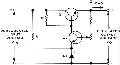
Fig. 1 - In the simple series-pass fixed-voltage regulator transistor Q1 controls the regulated output voltage, Vo. An ideal voltage-regulated power supply has zero output impedance so that the output voltage remains constant for any load current requirements. But, zero output impedances cannot be achieved, although supplies with impedance levels of a milliohm can be constructed. And, too, semiconductor device characteristics place a limit on the current and voltage that can be supplied to a load. Two simple series-pass voltage regulators are shown in Figs. 1 and 2. Transistor Q1 in each of these circuits controls the output voltage; thus the collector-emitter voltage rating of Q1 determines the maximum input-to-output voltage. All the current delivered to the load passes through Q1. Therefore, the power dissipated in Q1 is (Vin-Vout) times ILoad. If high input voltages and low output voltages and/or large load currents are necessary, it is possible that Q1 will have to dissipate large amounts of power. Obviously, under these conditions the regulator efficiency is low and the power rating (for the particular heat sinking) limits regulating capacity. For limited load variations, Q1 can be shunted by a resistor, thus shifting some power from Q1 to the resistor. The output voltage of the circuit (Fig. 1) is the Zener voltage minus the base-emitter voltage of Q1. R1 must provide enough current to the base of Q1 and to D1 to keep the voltage of D1 above its knee at all times. If the temperature characteristic of D1 is equal and opposite that of the base-emitter junction of Q1, the output voltage will remain constant with temperature. When variable output voltages are required, a circuit similar to that of Fig. 2 can be used. Here, the lowest possible output voltage is the breakdown voltage of D1 plus the base-emitter voltage of Q2.
Fig. 2 - In this variable-voltage series-pass regulator, transistor Q2 and a potentiometer are used to set voltage level.
Fig. 3 - This variable-voltage supply has overcurrent protection. Maximum output voltage is limited by the changes in the unregulated input plus the drive requirements of Q1. R1 provides the bias current for D1 whose voltage is compared to that at the potentiometer arm. If the load increases and causes the output voltage to drop, Q2 conducts less and Q1 conducts more, restoring the voltage to the original level. Basically, series-pass regulators are current, voltage, and power limited; and the circuit's control transistor must always be run in the safe operating area - region where there is no danger of secondary breakdown. However, series-pass regulators do provide extremely good regulation, fast response time, low output impedance, and low ripple. Their performance is almost independent of input frequency fluctuations and they have excellent dynamic response. They also provide variable output voltages and are readily adaptable to remote voltage sensing, remote programming, and current limiting or current regulating applications. The circuit output is virtually transient free. Overcurrent Protection The circuit shown in Fig. 3 is a regulated power supply with overcurrent protection and an output of 11 to 32 volts d.c. The maximum output current with the specified circuit components is 700 mA. The diode bridge consisting of D1 through D4 provides full-wave rectification of the 25-volt secondary of T1. Capacitor C1 is used to filter the rectified current and keep a positive voltage on the collectors of Q1 and Q2. Resistor R1 and capacitor C2 further reduce the ripple to maintain a stable d.c. voltage as a collector supply for Q3 and Q4, and for driving the base of Q1. Transistor Q2 is the series-pass device which regulates the output voltage. The resistor divider, R4-R5-R6, forms a sensing network. The voltage at the arm of potentiometer R5 is applied to the base of Q4, which compares the voltage to that of Zener diode D5. (Continued on page 78) The difference between the two voltages determines how much Q4 conducts. If the output voltage increases, the base voltage of Q4 increases and pushes it farther into the conduction region. This reduces the base current of Q1, which in turn reduces the current through Q2, lowering the output voltage. If the output voltage drops, Q4 moves toward cut off and Q1 and Q2 turn on. This increases the output voltage. In essence, the circuit is a feedback amplifier which tries to maintain the output voltage at a constant level independent of load condition.
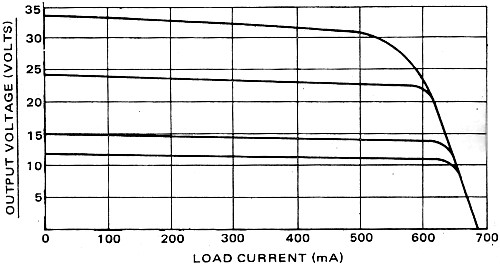
Fig. 4 - Voltage output versus load current for the circuit of Fig. 3.
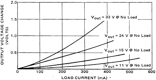
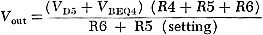
Fig. 5 - Regulation versus load current for the circuit shown in Fig. 3. The output voltage is determined by the potentiometer setting according to the following equation:
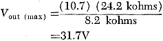
If R5 is set at the low end (A), the output is maximum and is given by:
The minimum output voltage (11.2 V) occurs when the arm of R5 is set to the high side (B). The regulation is a function of the potentiometer setting since this determines the amount of feedback. The closer the base of Q4 is to the positive output the greater the feedback. Overcurrent protection is provided by R2 and Q3. Since R2 is in series with the output, the voltage across it is proportional to the output current. This voltage is used to drive Q3 so that the larger the output current becomes, the more Q3 conducts. When Q3 is turned on, the base drive is removed from Q1 and this turns off power regulator Q2, thus limiting the output current. In this example, component values were chosen to limit the maximum current to approximately 700 mA. Fig. 4 shows the effectiveness of the current limiter. Load regulation at several output voltage levels is shown in Fig. 5. The overcurrent actually degrades the performance of the regulator circuit, particularly at the higher current levels, since it decreases the base drive of Q1. The power stage transistors, Q1 and Q2, were selected for high gain at -55°C. This maximizes the voltage and current regulator's control. At maximum output voltage and at low temperatures, Q1 requires a base current of about 1 mA. R1 was selected to deliver approximately 2.5 mA. This sets the minimum voltage regulator current in Q4 (MPS6531) at 1.5 mA, when the current regulator is not working. When the current regulator Q3 (2N4921) comes on, it must handle this current. For the opposite condition at high temperatures and low output voltages, R1 provides about 25 mA maximum current. The drive requirement for the power stage is not critical here, but Q3 and Q4 must be able to handle this current for effective control. The maximum temperature at which the circuit will operate is set by the heat sinking of Q1 and Q2. If these transistors are mounted directly to a heat sink and a good silicone grease is used, then the worst-case temperature rise above the temperature of the heat sink for Q2 is 25°C, while that for Q1 is about 20°C. Since the maximum operating temperature of Q1 is 150°C, this means the heat-sink temperature must be kept less than 130°C.
Posted December 25, 2017 |
|