The Solid-State Inductor
|
|
If you do a search on solid state inductors, you will not find much with a date later than the time when this article appeared in Electronics World in 1969. It appears a patent was issued in 1965, but the concept seems to never have caught on. The theory and construction is simple enough according to the information here. Fundamentally, it involves exploiting the properties of a Hall device when loaded with capacitive or inductive loads to effect inductive or capacitive properties, respectively. The ability to integrate capacitive elements into solid state substrates means the current and voltage phase relationship of an inductor can be obtained in an IC without a physical inductive element. Evidently practical implementation was difficult. The Solid-State Inductor By David L. Heiserman
Fig. 1 - Current flows lengthwise through a thin slice of semiconductor material. A magnetic field cuts the flow of current carriers at right angles and creates a Hall voltage along the edges of the semiconductor material as shown.
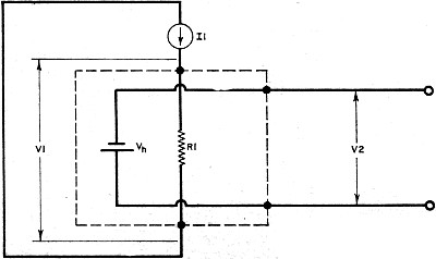
Fig. 2 - Equivalent circuit of unloaded Hall device. In the case of a Hall-effect device with very large impedance (or open circuit) across output terminals, the longitudinal voltage across the Hall material, V1, is simply the input current times the intrinsic d. c. resistance of the material, R1. Since the Hall voltage, Vh, delivers virtually no current to a very high impedance load, then voltage V2 equals Vh.
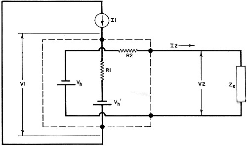
Fig. 3 - Equivalent circuit of loaded Hall device. When loaded with a fairly low impedance, Ze a Hall current I2 flows through the intrinsic transverse resistance, R2, and the external circuit. Since this current is subjected to the same Hall phenomenon as I1, the Hall current creates a secondary Hall voltage, V'h, that tends to oppose input current.
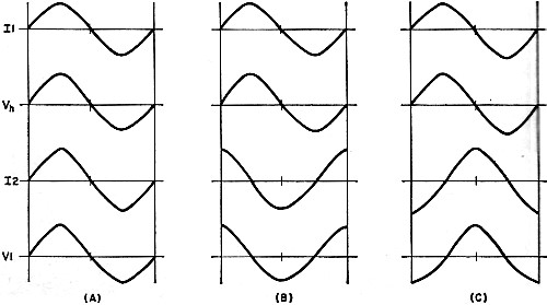
Fig. 4 - Phase relations between voltages and currents in a.c.-operated Hall device. In (A) the device is resistively loaded and all waveforms are in phase. In (B) a pure capacitance has been connected across the output terminals. The Hall current, I2, leads its source voltage, Vh, by 90 degrees. This voltage lag is reflected in the secondary Hall voltage which is mainly responsible for the V1 potential. As shown, the voltage across the input of the device leads the applied current by 90 degrees - just like an inductor. In (C) the device has been loaded with a pure inductor. The device now behaves as capacitor to input. By combining the Hall effect with integrated circuit technology, a solid-state device with inductive reactance has made its appearance. Conventional thinking about inductors seems to rule out any possibility of developing solid-state versions of inductive devices. Dr. S. Kataoka and his coworkers at the Tanashi Electrotechnical Laboratory in Tokyo, however, departed from conventional thinking recently and produced what may be the first practical approach to truly solid-state inductors. Semiconductor Hall-effect devices have been playing an increasingly important role in electronics technology for over a decade. Dr. Kataoka and his staff took advantage of some little-used Hall-effect phenomena to develop their new device. The Hall Effect Fig. 1 shows the basic experimental arrangement for demonstrating the Hall effect. A current, Ii, from a constant-current source passes lengthwise through a thin slice of semiconductor material such as indium antimonide (InSb). A magnetic field, B, at right angles to the input current bends the current carriers toward one edge of the Hall device. With an excess of charge carriers thus gathering on one edge, a potential difference, Vh, develops between the edges. This potential is the Hall voltage, and is given by the equation: Vh = KIiB sin θ; where K is the Hall constant, and θ is the angle between the input current and the magnetic field. The Hall constant depends upon the density and mobility of the current carriers, and the thickness of the Hall device. If the magnetic field is fixed and at right-angles to the input current, the Hall output voltage is proportional to the input current. Likewise, holding the input current constant and changing the strength of the magnetic field varies the Hall output voltage accordingly. The latter effect is employed in the design of Hall-effect gaussmeters. Fig. 2 shows the equivalent circuit for a Hall device with very large impedance connected across the output terminals. The input impedance of a Hall device with a large output load can be approximated by the simple relationship: Zi + R1. Used in this way, the input impedance of the Hall device is simply the inherent longitudinal resistance of the Hall material. Most present-day Hall devices are used in this mode. Short-circuiting the output terminals or making the load impedance very low, however, produces quite a different input impedance (Fig. 3). Making Ze very small makes the input impedance approximate: Zi = R1 + K2B2/R2. With the Hall output terminals short-circuited, then, the input impedance rises and responds to the square of the magnetic field strength. Such a device is used as a magnetoresistance - an effect just now becoming popular in research and development laboratories. Hall Devices with A. C. Inputs Fig. 4A shows the phase relationships between I1, Vh, 12, and V1 for a Hall device with a purely resistive load. Taking the constant-current input as a reference phase, the figure shows that Vh is in phase with I1. The Hall current developed by Vh is also in phase with the input as is the resulting voltage across the input terminals of the Hall device. Since the voltage across the device, V1, is in phase with the input current, the resistively loaded Hall device appears to be a purely resistive load to its associated current source. If the external load is purely capacitive, on the other hand, current through the external load will lead the Hall voltage by 90°. The result of this phase shift, as shown in Fig. 4B, is that the voltage across the input terminals leads the input current by 90°. Thus, with a capacitor across the output terminals, a Hall device appears inductive to the current source. On the other hand, connecting an inductor across the output terminals, as shown in Fig. 4C, makes the Hall device appear capacitive to the input current source. The Kataoka SSI Once it was established that a Hall device could simulate an inductor by connecting a capacitor across its output terminals, Kataoka carried the circuit idea one step further and integrated the capacitor into the Hall-effect device. The Kataoka SSI (solid-state inductor) consists of two thin slabs of InSb - one of the p-type and the other of the n-type - separated by a thin layer of a metal oxide dielectric. With a permanent magnet fixed to the device, the two slabs of InSb act as plates of a capacitor, and the voltage across the input terminals leads the input current, as illustrated earlier in Fig. 4B. Of course the metal-oxide capacitor is not perfect, and the internal resistance and Hall constant tend to limit the "Q" of the SSI. One of Dr. Kataoka's early inductors has a nominal inductance of 570 μH, and a "Q" factor of 0.37 at 1 kHz. By conventional choke standards this is, indeed, a poor inductor. Dr. Kataoka is quick to point out, however, that future improvements in design will soon increase the SSI performance to the point that it may become a major breakthrough in integrated-circuit technology. Editor's Note: For readers who are interested in further information on the Hall effect and on instruments that utilize this effect for magnetic measurements, refer to the article "The Hall Effect" by John R. Collins which appeared in our April, 1963 issue.
Posted August 17, 2017 |
|