|
February 1967 Electronics World
 Table
of Contents
Table
of Contents
Wax nostalgic about and learn from the history of early electronics. See articles
from
Electronics World, published May 1959
- December 1971. All copyrights hereby acknowledged.
|
A tetrode transistor is
technically any transistor than contains four active terminals. The tetrode transistor is more
commonly known today as a dual base bipolar junction transistor (BJT) or a dual gate
field effect transistor (FET or MOSFET). This 1967 Electronics World
magazine article reports on what was at the time a relatively new technology.
Common applications include feedback circuits for automatic gain control (AGC),
oscillators, and frequency conversion mixers.
The New Tetrode Transistor
By Joseph Tartas
By adding another base connection to a conventional triode transistor, two control
elements are provided. This unique advantage offers a great deal of circuit simplicity
in formerly complex semiconductor circuits.
The tetrode transistor has been around for almost fifteen years but unfortunately
has not attracted circuit designers as much as the more familiar triode transistor.
Because of the current interest in the FET (field-effect transistor), investigation
is being conducted into the unique advantages of this extra-element transistor and
the circuit simplicity it affords.
In this case, the exact equivalent circuit is difficult to illustrate. However,
one manufacturer presents it as an ideal transistor with the base-to-base resistance
as an external component as shown in Fig. 1B, which could be better represented
as illustrated in Fig. 1C. It is important to the working concept of the tetrode
that the equivalent circuit representation show three facts. (1) The base-to-base
resistance is a fixed ohmic resistance (except for larger than normal base currents).
(2) The resistor divider action in the equivalent circuit is for a.c. only. (3)
Most significant is the fact that the emitter and collector currents remain substantially
constant for the entire range of minimum to maximum signal gain. While the latter
is not true for the FET, the matter of the amount of signal modulation still holds
true in essence.

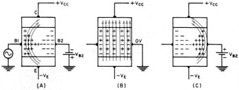
Fig. 1 - (A) A tetrode transistor has two base connections.
(B) and (C) Versions of the transistor equivalent circuit. Mechanically, the tetrode
transistor is built as shown in Fig. 1A. It greatly resembles the conventional
triode transistor, with the exception of a second base connection.

Fig. 2 - How base 2 applies a.g.c. to device. (A) With base
2 negative, base 1 controls electron flow. (B) With base 2 at zero volts, gain is
about unity. (C) With base 2 positive, base 1 has very little influence on the electron
flow.
To further clarify this, we must examine the base layer of the bipolar tetrode
in relation to the signal path and emitter-collector current. Fig. 2 demonstrates
the way in which tetrode action is obtained and the means by which the base 2 voltage
controls the signal gain of the transistor while the collector current remains substantially
constant.
In Fig. 2A, the arrows indicate the flow of electrons (in the case of the
n-p-n tetrode) near the base 1 area of the base layer due to repulsion by the negatively
charged base 2 end. This configuration represents the circuit under maximum gain
conditions, with base 1 grounded for d.c. (common base) and the emitter grounded
for a.c. (common emitter). Because of the resistance between the base connections,
the base layer will have a maximum negative charge at the base 2 end, with the charge
decreasing toward the base 1 end, so that in the narrowly confined area of base
1, the charge is all positive relative to both emitter and base 2. With such a charge,
the emitted electrons are repelled by the negative base 2 charge and attracted by
the positive base 1 charge. Under these conditions, all of the collector current
(which is essentially all of the emitter current) flows through the base 1 region
and is modulated by the incoming signal.
As the negative base 2 voltage is decreased (toward zero voltage), less of the
electrons are repelled by base 2, and at zero volts the electrons flow randomly
across the entire emitter-base-collector junctions shown in Fig. 2B. When this
occurs, only a small amount of current flows near base 1 and hence only a small
amount of signal modulation appears at the collector. Such a condition might represent
a gain of unity or less.
If the base 2 voltage is allowed to reverse polarity and become positive by a
small amount (relative to base 1) as shown in Fig. 2C, then the emitted electrons
are repelled by the base 1 charge and essentially all of the current flows in the
base 2 region. This state is minimum gain and actually represents attenuation of
the incoming signal by 20 dB or more.
It is interesting to note that the linearity of the base-to-base resistance is
dependent to a large degree on the amount of emitter current as well as the level
of the base-to-base current. Because the tetrode transistor is intended for small-signal
applications only (and hence a small emitter current), the base-to-base resistance
is normally used within its linear characteristics, and it is just these characteristics
that lend themselves nicely to r.f. and i.f. circuitry. For the transistor, there
is practically no change in collector current and hardly any change in base current;
therefore, there is essentially no change in input capacitance or loading. Because
of this, the response of the amplifier does not shift or skew as the stage gain
is radically reduced. The Miller effect, commonly encountered in vacuum tubes, is
thus eliminated.
Since the total base 1 current is the sum of the base 1-emitter current and the
base-to-base current, there is very little change in bias with an alteration in
base 2 control voltage.
Because of the isolation provided by the second base, the need for neutralization
is greatly reduced in the tetrode. Since the nature of feedback is analogous in
both tubes and transistors, similar methods of compensation are possible in either
case. However, for tetrode transistor circuitry, it is only in rare cases that the
maximum potentialities of a tetrode circuit can be improved solely through neutralization.
Tetrode Circuits
The tetrode is useful only in small-signal applications, in most cases the application
is at r.f. frequencies where convenience of the second base may be used to best
advantage. Examples include a.g.c.-controlled i.f. stages; converters where the
second base becomes a separate injection element; r.f. signal generators with the
output level controlled through the second base; and either an r.f. video attenuator,
when used as a variable impedance directly across a line.
While potential applications are unlimited, the familiar transmitter and receiver
circuitry are easily adaptable to use of the tetrode, whether the transistor is
bipolar or FET.
At the present time, the only bipolar tetrodes available are the 3N34 and 3N35,
both manufactured by Texas Instruments. However, the more recently introduced FET
tetrodes are beginning to appear in greater numbers each month. Nearly all the leading
transistor (and also tube) manufacturers have tetrode FET's in their current transistor
listings, There is also evidence that some companies are planning to produce pentode
transistors by similar techniques.
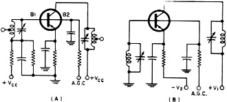
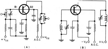
Fig. 3 - (A) Circuit using a single positive supply source.
(B) Similar circuit uses dual voltage supply to provide grounded base 1 circuit.
This simplifies r.f. grounding.

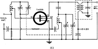
Fig. 4 - Circuit configurations for tetrode transistors.
(A) FET 45-MHz i.f. amplifier shows how a.g.c. is applied.
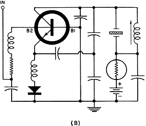
(B) A crystal-controlled FM oscillator.
(C) Simplified autodyne converter uses both gates of FET transistor.
Without going into a discussion of the field effect vs. holes or electrons, it
is interesting to find that the dual-gate FET (or tetrode), although different in
physical construction, still obtains a variable gain control by a method similar
to that of the bipolar tetrode. The FET, however, unlike the bipolar transistor,
has a variable drain current (equivalent to the collector current) with a change
in a.g.c., just as in a vacuum tube. The big difference is that there is little
or no change in input capacitance with a.g.c., nor is there any significant change
in input loading, in spite of the current change,
Powering Tetrodes
The FET is operated in a manner that is similar to that of both the vacuum tube
and the bipolar grown-junction tetrode, except for the aforementioned differences.
The bias may be derived from a divider where feasible, or a grounded-base (or gate)
circuit may be used where preferable, as shown in Fig. 3. While the single
supply of Fig.
3A is similar to that of the vacuum-tube circuit using a.g.c., it must be remembered
that the separate base element of the transistor is used for that purpose. For high-frequency
applications, it may be more desirable to return input circuits directly to ground,
as shown in Fig. 3B, supplying negative bias to the emitter. This configuration
is described as common base for d.c. and common emitter for r.f. (through the emitter
bypass capacitance). The resistor-capacitor network in base 2 lead is used only
as a filter.
A.G.C. Supply
The a.g.c. voltage is usually derived from the detector circuit of a receiver,
although in other types of equipment, it may be more elegant. Whatever the source,
its prime purpose is to keep the output level of the stage or stages at a constant
level over an extremely wide range of input levels.
The bipolar transistor literature originally recommended a constant-current source
for the second base, but it was found that the voltage source for the required base
current could be controlled with a less complicated circuit, with more standard
results from unit to unit.
FET tetrodes require only a voltage source, with maximum gain occurring at zero
volts on the second gate, at least for those elements used for a.g.c. action. All
in all, the basic ideas used in either transistor or vacuum-tube a.g.c. are quite
similar. The only precaution involved in the a.g.c. voltage is that it should be
kept within the recommended limit, as breakdowns occur beyond this limit that can
permanently damage the transistor.
Applications
Fig. 4 shows a number of typical applications of the tetrode transistor.
Fig. 4A, a 45-MHz amplifier using an FET, shows a gain of 20 dB and an approximate
a.g.c. range of 40 dB for a change of zero to 6 volts on gate 2. This gate may be
returned to a fixed voltage source of 6 volts through a potentiometer for manual
gain, or it may be returned to ground or to base 1 for a fixed gain with no control.
The crystal-controlled oscillator of Fig. 4B is frequency-modulated by applying
a reverse a.c. current to base 2, thus causing a characteristic change in the output
capacitance that shunts the crystal and tuned circuit.
In a similar application with a v.f.o. (non-crystal controlled), a 250-kHz swing
was achieved for a center frequency of 750 kHz for a base 2 current of 150 to 200
μA.
An old favorite, the autodyne converter, has been modernized in Fig. 4C
by using the two gates of an FET as separate injection elements for input and local
oscillator signals.
Because of the control action exerted by the introduction of the second base
element, there is almost no limit to the variety of possible applications for tetrode
transistors. Automatic level controlled generators, variable load impedances, a.f.c.
circuits, and switch able r.f. amplifiers are only a few of those that have been
successfully developed.
Posted July 29, 2021
(updated from original post on 2/5/2012)
|