|
September 1965 Electronics World
 Table
of Contents
Table
of Contents
Wax nostalgic about and learn from the history of early electronics. See articles
from
Electronics World, published May 1959
- December 1971. All copyrights hereby acknowledged.
|
I have to admit to only
having ever used a transistor curve trace in two instances. The first was while working
as an electronics technician at Westinghouse Oceanic Division in Annapolis, Maryland,
in the early and mid 1980s. We built sonar systems for the U.S. Navy, and when the
contract levels were really low, some of us would get farmed out to other parts
of the company rather than doing layoffs. On one occasion I spent about two months
sharpening drill bits and end mill bits in the machine shop. Another time I worked
at incoming inspection doing sample testing of resistors, capacitors, inductors,
diodes, transistors, etc. That is where I first used a transistor curve tracer.
The truth is at that point I didn't really know what the curves represented from
a performance standpoint. Since it was in the days before digital test equipment,
we had a plastic overlay on the display with upper and lower limits for the curve.
Test engineers wrote procedures and did equipment setup so really all you needed
to perform the tests was decent eyesight and a bit of good sense. The next time
I used a curve tracer was during laboratory experiments at the University of Vermont
(UVM) whilst working on my BSEE degree (graduated in 1989 at 31 years old - a late
bloomer). This article describing the use of a transistor curve tracer appeared
in a 1965 issue of Electronics World magazine. It was a lot of people's
introduction to transistor parameter testing and characterization.
Using a Transistor Curve Tracer

Fig. 1 - The author is shown using a transistor curve tracer
along with a thermocouple to check temperature effects on a transistor.
By Ralph E. Show / Instrument Engineering, Tektronix, Inc.
Operating principles of an important piece of test equipment which displays a
complete family of diode or transistor characteristic curves. The method of interpreting
curves to obtain parameters is covered.
Transistor curve tracer displays the dynamic characteristic curves of transistors
and semiconductor diodes on the screen of a cathode-ray tube. This article will
show some of the displays it is possible to obtain with a curve tracer and how the
displays may be used to determine transistor and diode parameters. These displays
are intended for measurements of transistor characteristics which exist well below
alpha cut-off, commonly measured between d.c. and 1000 cps, hence, we will not consider
any high-frequency measurements.
Fig. 1 shows a curve tracer being used with a thermocouple to check temperature
effects on a medium-power p-n-p transistor.
We have chosen to give examples of measuring the four hybrid or h. parameters
from the characteristic curves, although other parameters could be measured as well.
Further, we have given examples predominantly in the common-emitter configuration.
Measurements can also be made using common-base or common-collector circuits as
well, with either p-n-p or n-p-n transistors being employed.
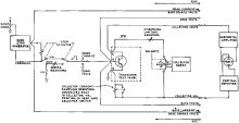
Fig. 2 - Functional block diagram of the Tektronix Type 575 transistor
curve tracer is shown here.
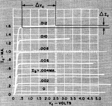
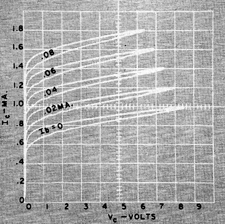
Fig. 3 - Forward current transfer ratio hfe(beta)
is determined by measuring the change in collector current produced by a change
in base current at a specified collector voltage. In this case at Vc
= 10v., beta = Δ|c/Δ|b = 1.6 div. X (2 X 10⁻¹)/12 X
10-6) = 1.6 X 102 = 160. Alpha = β/(β + 1) = 160/161 ≈
0.994. Curves shown are for "n-p-n" transistor in common-emitter configuration.
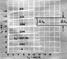
Fig. 4 - Output conductance, hoe, is determined by
measuring the change in collector current produced by a change in collector voltage
at a specified base current. At |b=0.012 ma., hoe = Δ|c/ΔVc
= 0.2(2 X 10⁻⁴)/(4 X 0.5) = 0.4 X 10⁻⁴/2 = 0.2 X 10-4 = 20 μmhos.
Curves are for "n-p-n" transistor, common-emitter circuit.
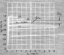
Fig. 5 - Input impedance, hie, is determined by measuring
the change in base voltage resulting from a change in base current at a specified
collector voltage. At Vc=5 v., hie=Δvb/Δ|b=
0.6(2 X 10⁻²)/10-5 = 1.2 X 103 = 1200 ohms. The
above curves are for "n-p-n" transistor in common-emitter configuration.
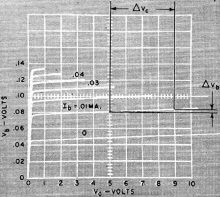
Fig. 6 - Reverse voltage transfer ratio hre, is determined
by measuring the change in base voltage resulting from a change in collector voltage
at a specified base current. In this case at 1b = 0.01 ma., hre
= ΔVb/ΔVc = 0.2(2 X 10⁻²)/4 = 1 X 10⁻³
or 1000 X 10-6 "N-p-n" transistor in common-emitter circuit.
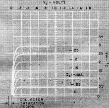
Fig. 7 - Collector family, "n-p-n" transistor, common-base circuit.
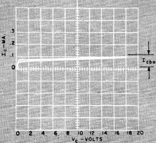
Fig. 8 - Measurement of |cbo, the collector current
that flows with emitter circuit open is shown on |c vs Vc
display for "n-p-n" transistor in common-base circuit. At Vc = 18 v.,
|cbo = 0.1 ma.
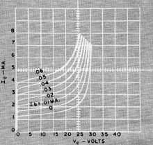
Fig. 9 - Collector breakdown characteristic curves of |c
vs Vc for various values of |b for "n-p-n" transistor in common-emitter
configuration. Note sharp rise of current around 25-30 volts Vc.
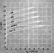
Fig. 10 - The loops in the characteristic curves shown here are
the result of the presence of collector-to-base capacitance. With reduced capacitance
the loops shown will close up.
Advantages of Curve Tracer
The visual display of a family of transistor characteristic curves using oscilloscopic
techniques, employing synchronously stepped and swept voltage-current sources, offers
certain advantages over the d.c. point-to-point measurement techniques:
1. Small irregularities in the characteristics, which may escape observation
by the point-by-point method, are readily visible.
2. The extremes in the variation of a parameter value may be observed without
altering the operating conditions of the transistor.
3. The changing magnitudes of two parameters may be observed simultaneously,
as well as the dependence of one upon the other.
4. The short duration and lower duty cycle of the peak sweeping voltages or currents
applied to the transistor pro-duce less thermal rise than does the steady-state
d.c. condition which occurs in point-by-point measurements. Inaccuracies due to
thermal gradients are thereby minimized.
5. For the same reason noted in (4), the maximum ratings of the transistor may
be observed without exceeding the safe limit of its power dissipation; thus incipient
junction-break-downs are minimized.
6. Observation, comparison, or a permanent record by photographic techniques
of the transistor characteristics may be made more rapidly than by the point-by-point
plot, thus affording a savings in manpower.
7. A resistive load line may be constructed in the family of characteristic curves
so that dynamic performance data for the transistor may be forecast.
Transistor characteristic curves may be found to deviate more widely from the
published "nominal" characteristic curves than those for vacuum tubes. For this
reason, the curves obtained on a curve tracer may not always agree with curves published
in data sheets or transistor manuals.
Curve-Tracer Operation
A functional block diagram of the Tektronix Type 575 transistor curve tracer
is shown in Fig. 2. In this curve tracer, two signals are developed to be applied
to the transistor. One signal consists of either constant-current or constant-voltage
steps, which are normally applied to the base (common-emitter configuration), or
to the emitter (common-base configuration). The other signal is a variable amplitude
half-sine wave, normally applied to the collector. The two signals are synchronized
so that for the duration of one step, or one-half step, there is one excursion of
the half-sine voltage from zero (ground) to maximum and back to zero.
The base step generator produces from 4 to 12 steps in selected amplitude increments
of constant current or constant voltage. The duration of each step is either 1/20th
or 1/240th of a second. The steps may be made repetitive, to occur once, or made
inoperative and held at zero step level. The steps may be positive (for n-p-n) or
negative (for p-n-p) in polarity with the zero step value adjustable by a small
amount, positive or negative, from ground to start the stair-steps on the zero-volts
or zero-current input curve.
The output of the base step generator is fed through a switch to the base (B)
terminal of the test panel. The switch provides a means of disconnecting the base
terminal from the base step generator to either open or short the terminal to ground.
The collector sweep is the source of the half-sine collector sweep voltage. The
peak collector sweep voltage is variable in amplitude from zero to 20 volts at 10
amps, or zero to 200 volts at 1 amp. The polarity of the half-sine shaped voltage
excursions may be made positive (for n-p-n) or negative (for p-n-p) from ground.
The duration of sweep from zero to maximum and back to zero is always 1/120th of
a second.
The collector supply may be fed directly to the collector terminal (C) of the
test panel, or variable dissipation-limiting resistance values may be inserted.
The third terminal (E) of the test panel is ground. The test panel (not entirely
shown in Fig. 2) has a switch for transferring all connections from the left-hand
terminals and socket to the right-hand terminals and socket with a neutral "off"
position. Another switch is provided to switch the sockets only from grounded base
to grounded emitter.
The horizontal amplifier may be connected to display one of four signals on the
horizontal axis of the cathode-ray tube: (1) collector volts; (2) base volts; (3)
base current; (4) an external signal. In the same manner, the vertical amplifier
may be connected to display one of four signals on the vertical axis of the CRT:
(1) collector current; (2) base volts; (3) base current; (4) an external signal.
Display Considerations
The most common transistor display is a "collector family," such as shown in
Fig. 3. In this display, collector voltage Vc is plotted horizontally,
collector current Ic is plotted vertically, and each curve or step represents
a different value of base current Ib. Such a display is obtained by connecting
the transistor under test for the normal operating polarities, that is, for a forward-biased
emitter and for a reverse-biased collector.
However, with the curve tracer, the polarity of the base step and collector sweep
signals may be selected independently and used to advantage. For instance, the emitter
may be reversed-biased in order to measure the amount of current or voltage required
to decrease the collector current, Icbo or Iceo, to minimum
value.
A given parameter may be measured from anyone of the displays containing the
current and voltage relationships involved in the parameter. The display chosen
depends upon the particular parameter and the characteristics of the transistor
under test. The display that should be used is, of course, the one which yields
the most accurate measurement or vivid display of that parameter.
The user may sometimes prefer to measure other parameters that may be combined
in a formula to produce a more accurate end result. A typical case is the relationship
between a (alpha), the common-base forward current transfer ratio and β (beta),
the common-emitter forward current transfer ratio. In the common-base configuration
of Fig. 7, for example, it can be seen that the change in collector current for
a given change in emitter current is very close to one. In a common-emitter configuration,
however (Fig. 3), the change in collector current is considerably more than the
change in base current. Since α and β are related by α = β
/ (β + 1), we may find β to a greater degree of accuracy as far as scaling
is concerned, and solve for a.
A word may be in order regarding small-signal hybrid, or h, parameters. In small-signal
operation, linearity should exist over the operating range of the parameter and
the value of the parameter should be independent of the signal amplitude. Ordinarily,
the active region of a transistor without defects is quite uniform, and a cursory
examination of the family of " characteristics will verify that linearity exists
over the operating range of the parameter.
The versatility of the curve tracer provides for making "small-signal" as well
as "large-signal" measurements. In order to verify that the parameter value, or
operating region, of the transistor is independent of the signal amplitude, additional
measurements of the parameter may be made adjacent to, or within, the intended operating
region and the resulting values compared. For instance, the base step values may
be reduced and the number of steps increased to examine a smaller segment within
the same operating region, etc.
The waveforms, Figs. 3 through 6, illustrate some of the displays it is possible
to obtain with a curve tracer and measurements that can be obtained from the displays.
These show characteristics of a small-signal n-p-n transistor in the common-emitter
mode, and how parameters may be obtained.
Common-Base Configuration
The parameters for the common-base or common-collector configurations may be
handled in the same manner as just illustrated for common-emitter configuration.
From observation of the collector family of output characteristics in common-base
configuration, shown in Fig. 7, it is clear that hƒb or α,
which equals ΔIc/ΔIe, and hob, which
equals ΔIc/ΔVc, are difficult to scale from the graticule.
This is quite normal and it may be anticipated that variations between transistors
will not appear as vividly as they would in common-emitter operation.
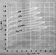
Fig. 11 - Same display as shown in Fig. 10 except in this case
a 1000-pf. capacitor was added externally between base and collector.
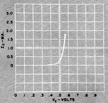
Fig. 12 - The zener diode forward conduction characteristics.
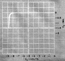
Fig. 13 - Zener diode reverse breakdown characteristics. The
zener control voltage is shown to be approximately 8.7 volts.
The curves of Fig. 7, by themselves, are principally informative in the "saturation
region," which appears to the left of zero collector volts. It will be recalled
that in common-base configuration, unlike common-emitter, the polarity of the emitter
is opposite to that of the collector. The apparent forward biasing of the collector
in the "saturation region" results from emitter current and hence appears opposite
in polarity to the applied collector voltage. Its magnitude may approach the magnitude
of the emitter voltage; however, it can never exceed this value of voltage.
Collector Cut-off & Breakdown
The collector current which flows with zero emitter current (common base) Icbo,
or with zero base current (common emitter) Iceo may be measured directly
from the collector family of curves. A typical measurement for Icbo is
illustrated above in Fig. 8.
As the voltage is increased on a reverse-biased collector of a transistor, a
point will be reached where the collector current increases rapidly and may become
essentially independent of the collector voltage. Several measurements of the break-down
characteristics may be obtained with a curve tracer, but in this article we will
not attempt to differentiate among the phenomena referred to as avalanche, punch-through,
zener breakdown, or carrier multiplication, since they are largely dependent upon
the configuration, type, and geometry of the transistor.
Collector breakdown is shown in Fig. 9, where I, increases almost without limit
in the vicinity of 25 to 30 volts on the collector (Vc) .
Under certain conditions, some transistors will exhibit a negative-resistance
characteristic in the breakdown region. Oscillation may also occur in some other
region of the characteristic curve and may be recognized by the faint and ragged,
or erratic, behavior of the trace on the oscilloscope dis-play on the curve tracer.
Collector-Capacitance
The effect of the collector capacitance may become quite pronounced in some transistors.
The loop resulting from the collector-to-base capacitance causes a displacement
current to add and subtract from the current of the transistor. The effect is most
pronounced in common-emitter configuration with low base drive, high collector voltage,
and the greatest expansion of the vertical collector-current display. The capacitance
effect is more pronounced at the knee of the curve in the collector family because
of the sudden change in collector current in the transistor. At the same time, the
rate of change of the collector half-sine shape sweep voltage is maximum, that is,
near the beginning and near the ending of the particular operating cycle. The equivalent
steady-state d.c. value of collector current may be established by decreasing the
collector voltage until only the peak of the collector sweep occurs at the point
in question. The approximate magnitude of the capacitance may be measured by adding
a capacitor of 10 to 1000 pf. between the base and collector terminals. The transistor
capacitance is approximately equal to the capacitance of the external capacitor
when the vertical size of the loop is doubled. A comparison of Figs. 10 and 11 illustrates
the effects of the collector-to-base capacitance.
Diode Characteristics
Forward-conduction or reverse-voltage breakdown of a diode may be displayed on
a curve tracer by the simple expedient of using the collector sweep supply as a
voltage source. The display will represent the E-I plot with anode current plotted
vertically as Ic, and the anode voltage plotted horizontally as Vc.
Forward and reverse zener diode characteristic curves are shown directly below in
Figs. 12 and 13 respectively.
Posted July 27, 2022
|