|
June 1969 Electronics World
 Table of Contents
Wax nostalgic about and learn from the history of early electronics. See articles
from
Electronics World, published May 1959
- December 1971. All copyrights hereby acknowledged.
|
Like most people familiar
with electronics, when negative resistance semiconductors are mentioned, I immediately
think of tunnel diodes.
Negative resistance is the characteristic where in increase in voltage across
the p-n junctions results an a decreased current. Although the tunnel diode
was invented by by Leo Esaki (Sony) in 1957, it is not mentioned anywhere in
this 1969 article. Instead author Wesley Vincent (Motorola) describes the theoretical
operation of 4-layer (3 junction) semiconductors and how they can be biased
to mimic true negative resistance devices. Given that one of the most common
applications of tunnel diodes is to construct relaxation oscillators, knowing
which configurations of standard BJTs can act like negative resistance devices
might help explain unintended high frequency oscillations in some amplifier
circuits.
See also "The
Tunnel Diode" from a 1960 issue of Popular Electronics.
Using Transistors as Negative-Resistance Devices
By Wesley A. Vincent / Advanced Development Section
Government Electronics Div., Motorola Inc.
 By using simple transistor-resistor combinations,
characteristics of four-layer diodes, SCR's, and UJT's may be readily simulated. By using simple transistor-resistor combinations,
characteristics of four-layer diodes, SCR's, and UJT's may be readily simulated.
Several rather unusual negative-resistance devices have become available
to the circuit enthusiast during the past few years. These devices include four-layer
diodes, silicon controlled rectifiers (SCR's), and unijunction transistors (UJT's)
to name a few of the most popular. Industrial competition and improved manufacturing
and production techniques have resulted in price reductions, allowing those
with limited budgets to use them in circuit projects. However, ordinary transistors
are more likely to be readily available for circuit experiments. By using the
simple transistor-resistor combinations presented in this article, the characteristics
of four-layer diodes, SCR's, and UJT's may be simulated.
A relaxation oscillator using the analog circuit of the unijunction transistor,
which is quite similar in operation to the unijunction relaxation oscillator,
is also described. Although the test results presented were obtained using silicon
transistors, low-leakage germanium transistors may be substituted.
An advantage gained in simulating these negative-resistance devices is that
the more important device parameters may be determined by selecting transistors
and resistors used in the substitute combinations. The basic building block
for the circuits discussed is based on the operation and theory of the four-layer
or p-n-p-n diode. The SCR and UJT are then presented as extensions of the four-layer
diode in theory and in synthesizing their characteristics, using transistor-resistor
combinations.
Four-Layer Diode Theory
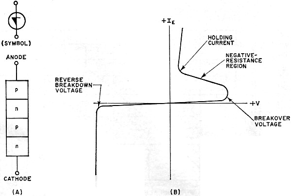
A four-layer diode consists of four alternate regions of p- and n-doped semiconductor,
as shown in Fig. 1A. The p-region terminal is called the anode while the
n-terminal is referred to as the cathode. The V-I characteristics and parameter
definitions associated with the device are shown in Fig. 1B. With the anode
biased positively with respect to the cathode, a negative-resistance (current
increases as the voltage decreases) region exists. The four-layer diode may
also be represented by a regenerative transistor feedback arrangement consisting
of a p-n-p and n-p-n transistor, as shown in Fig. 1C.
Using this model, the mathematical expression for the terminal current IE,
may be expressed in terms of the transistor parameters as follows:
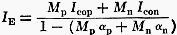
where αp
and αn
are the common-base current gains; Icop and Icon are the
collector-to-base leakage currents; Mp and Mn are the
multiplication factors which account for carriers created by impact ionization
in a reverse-biased junction during breakdown.
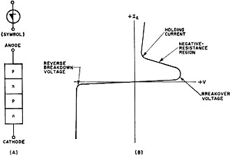
Fig. 1A - Four-layer diode has four alternate "p, n"
regions and three "p-n" junctions. B - V-I characteristics
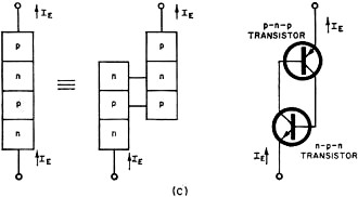
Fig. 1C - Transistor model.
The p and n subscripts refer to the parameters associated with the p-n-p
and n-p-n transistors, respectively, in Fig. 1C. Usually Mp
and Mn are assumed to be equal and are designated simply as M. If
the leakage terms are combined, the previous equation may be expressed in a
slightly more simplified form as:
This expression may be used to briefly explain the forward V-I characteristics
of the four-layer diode as follows: For anode-to-cathode voltage less than the
breakover voltage, only a small leakage current flows. The current-gain parameters
αp
and αn
are complex functions of injection efficiency, the base transport factor, and
surface conditions. For small anode-to-cathode voltages, the combined values
of αp
and αn
are much less than 1. Since no multiplication takes place at low voltages, M
is equal to unity. The denominator in the above expression is only slightly
less than unity so that IE is approximately equal to Ico.
The current gains
αp
and αn
increase with increasing current as the forward voltage is increased. Thus,
the forward current increases slightly with increasing voltage. As the forward
voltage is continually increased, the condition occurs where M (αp
+ αn
) = 1. When this occurs, the current increases sharply over the previous small
leakage current as shown in Fig. 1B. This voltage is known as the breakover
voltage. At the breakover voltage, multiplication (M) is greater than unity
since avalanche breakdown is occurring in the reverse-bias junctions. Therefore,
the combined value of
αp
and αn
is less than 1.
As the current increases beyond the breakover current,
αp
and αn
increase due to their current dependence. A lower multiplication (M) is then
required to maintain the breakover voltage. As a result, the forward bias across
the diode begins to decrease with a negative-resistance region occurring. The
current increases and voltage decreases until the holes injected at the anode
of the p-n-p transistor equal the electrons injected at the emitter of the n-p-n
transistor. This is a result of current continuity conditions and results in
forward bias of the center junction of the four-layer diode. The transistors
in the model are then in their "on" or saturated state.
In the reverse operating mode, the four-layer diode acts like two reverse-biased
diodes in series. A small reverse current exists until the breakdown condition
finally takes place.
Equivalent Circuit for Four-Layer Diode
When silicon transistors are connected in the manner shown in Fig. 1C,
the forward V-I characteristics resemble those of an ordinary p-n junction rather
than those of a four-layer diode. This occurs because the discrete transistor
current gains are much higher than the current gains in a four-layer diode.
The breakover condition of M (αp
+ αn)
= 1 is reached at a few tenths of a volt when current injection for the transistor
begins.
Large transistor leakage currents can also cause low breakover voltages.
One method of reducing the transistor current gain is to place a resistor between
its base and emitter terminals. A shunt path exists for the emitter current
with the result that very little injection takes place until the voltage across
the shunt resistor begins to forward-bias the base-emitter junction.
In the transistor equivalent model shown in Fig. 1C, several possibilities
exist for reducing the combined values of
αp
and αn.
Resistors can be inserted between the base and emitter of the p-n-p or n-p-n,
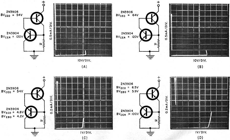
or both, transistors. Shown in Figs, 2A and 2B are the forward V-I characteristics
for a transistor-resistor equivalent circuit with a 1000-ohm resistor inserted
between the base and emitter of the n-p-n transistor. It can be seen from these
curve-tracer photographs that the forward V-I characteristics are similar to
those of the four-layer diode.

Fig. 2 - (A, B) The transistor-resistor equivalent
circuit for a four-layer diode. (C) Same but with inverted "n-p-n" transistor
and (D) with an inverted "p-n-p" transistor.
In the configurations shown, the breakover voltage is determined by the BVCEO
parameter of the p-n-p transistor. In general, the breakover voltage will be
determined by the transistor with the lower breakdown parameter. Shunt resistors,
used to reduce either
αp
or αn,
will increase the transistor breakdown voltage from BVCEO to BVCER.
In Figs. 2A and 2B, BVCEO for the n-p-n transistor is approximately
50 V. However, with the shunt resistor of 1000 ohms, the BVCER voltage
is greater than 100 volts; hence, the breakover voltage for the circuit is determined
by the p-n-p transistors with BVCEO voltages of 54 and 64 volts,
respectively.
For breakover voltages less than the BVCEO voltage of the transistors,
either the p-n-p or n-p-n transistor may be operated in an inverted mode. Results
for such a circuit are shown in Fig. 2C where the n-p-n transistor has
been inverted. Even though alpha for an inverted transistor is severely reduced,
it is still necessary to reduce the alpha of either the n-p-n or p-n-p transistor
with a shunt resistor. As with the previous circuit, the breakover voltage is
determined by the lower breakdown of the two devices. In this configuration
the breakover point is determined by the BVECO voltage of the n-p-n
transistor. (A close approximation of the breakover voltage is obtained by knowing
the more commonly specified BVEBO voltage of the n-p-n transistor.)
Another four-layer diode equivalent circuit with its forward V-I characteristics
is shown in Fig. 2D, where the p-n-p transistor has been inverted. The
BVECO voltage of the p-n-p transistor determining the breakover voltage
is 6.5 volts.
By selecting the transistor breakdown voltage, the experimenter can simulate
four-layer diode characteristics with a breakover voltage of 5 to 100 volts
or more.
The holding current for these configurations is determined by the transistor
current gains and shunt resistors. The holding current may be selected from
a few microamps to 10 or 20 mA or more. Decreasing the value of the shunt resistor
(and hence decreasing the transistor current gain) increases the holding current.
The reverse breakdown voltage for the four-layer diode equivalent circuit
is similar to that of a four-layer diode and is determined by the junction breakdown
of the transistors in the specific configuration. Note that if shunt resistors
are used to reduce both
αp
and αn,
the reverse breakdown voltage will be only approximately 0.65 volt, the voltage
of one forward-biased diode.
The most noticeable temperature effect for these configurations is that the
holding current decreases with increasing temperature. If the transistor alphas
are not reduced sufficiently by shunt resistors, it is possible for premature
firing to occur with increasing temperature as
αp
and αn
increase with temperature.
The test results are not unique for any particular transistor type. Similar
results have been obtained using other silicon and low-leakage germanium transistors.
Simulation of SCR Characteristics
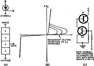
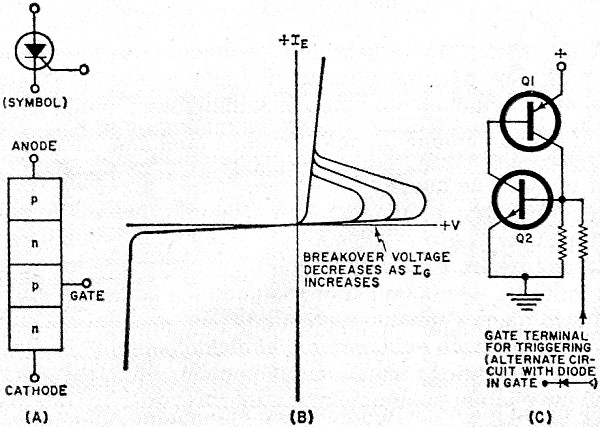
Fig. 3 - (A) An SCR is four-layer diode with gate terminal.
(B) V-I characteristics, and (C) equivalent circuit for SCR.
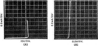
Fig. 4 - Characteristics of simulated SCR shown here
(A) in blocking state and (B) in "on" state due to 1 V on gate.

Fig. 5 - (A) Symbol and circuit used to explain operation
of UJT. (B) Forward V-I characteristics. (C) Equivalent circuit.
The SCR consists basically of a four-layer diode with the addition of a third
terminal called the gate. The gate is usually attached to the p-region near
the cathode, as shown in Fig. 3A. The gate terminal is used to switch the
SCR from the blocking or "off" state to a low-impedance or "on" state . As the
gate current increases, the breakover voltage decreases, as shown in Fig. 3B.
With a minimum gate current, which is dependent on the particular SCR construction,
the negative-resistance region no longer occurs and the V-I characteristics
resemble those of an ordinary p-n diode. In theory, the gate current causes
the individual current gains
αp
and αn
to increase so that the condition for breakover, M (αp
+ αn)
= 1, occurs prior to four-layer junction breakdown.
The transistor-resistor equivalent circuit for the four-layer diode may be
adapted to obtain SCR characteristics by simply adding the gate terminal with
a series resistor to the base of the n-p-n transistor shown in Fig. 3C.
The series gate resistor insures that the collector current of Q1 causes Q2
to turn on, leading to regenerative action and the low-impedance state. Otherwise
the collector current (electron current) of Q1 would flow into the gate terminal.
A diode may also be used to replace the series gate resistor in Fig. 3C.
Curve-tracer results for the simulated SCR are shown in Fig. 4, where
Q1 and Q2 were 2N3906 and 2N3904, respectively. Both resistors used in the equivalent
circuit were 1000 ohms.
Fig. 4B shows the equivalent SCR turned "on" by an applied gate voltage
of 1 volt. The exact gate voltage and current necessary for switching the simulated
SCR will depend on the transistors and resistors used in the equivalent circuit.
A gate current of 1 milliamp should be sufficient to switch silicon or germanium
combinations.
Simulation of the Unijunction Transistor
The unijunction transistor is another device with negative-resistance characteristics.
It is used in oscillators, timing circuits, pulse and sawtooth generators, and
special triggering applications. The unijunction equivalent circuit can be considered
to be a resistive n-type silicon bar with a p-n junction formed between the
terminals, as shown in Fig. 5A. The end terminals of the bar are referred
to as bases while the anode of the p-n junction is called the emitter. The resistance
between the two bases is known as the interbase resistance. The geometry of
the first unijunctions consisted of the bar structure although newer UJT's include
cube, planar, and p-base complementary structures.
In operation, the interbase resistors form a voltage divider with the voltage
applied between base terminals. When the voltage at the emitter forward-biases
the p-n junction, the unijunction enters the negative-resistance region. Forward
V-I characteristics for the unijunction, showing the negative-resistance region,
are illustrated in Fig. 5B.
The unijunction transistor can be considered to be a four-layer diode with
the addition of biasing resistors as shown in Fig. 5C. The biasing resistors
replace the interbase resistors of the unijunction and are used to set the break
over point. However, in unijunction terminology, this voltage is known as the
peak-point voltage. Also, the minimum holding current is referred to as the
valley current (IV) for the unijunction.
For commercially available UJT's, the ratio of interbase resistors setting
the peak-point voltage is determined by the semiconductor manufacturer. Using
the transistor-resistor equivalent circuit in Fig. 5C, the peak-point voltage
may be selected by choosing the appropriate resistive dividers, RI and R2.
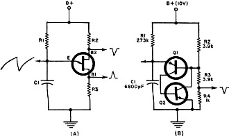
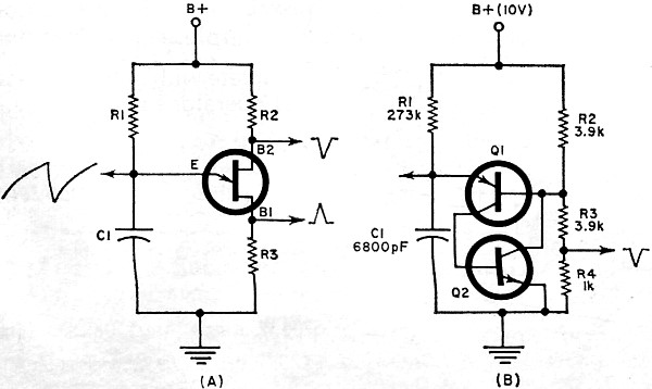
Fig. 6 - (A) UJT oscillator. (B) Equivalent-circuit
version.
A relaxation oscillator is one of the most common applications for the UJT.
The basic configuration appears in Fig. 6A. A positive pulse appears at
base 1, a negative pulse at base 2, and a sawtooth waveform at the emitter.
The frequency of oscillation is controlled by the R1C1 time constant; R2 is
selected for minimum frequency change over a given temperature range, and R3
limits the capacitor discharge current.
The basic operation of the relaxation oscillator is as follows: When "B+"
is applied, all of this voltage immediately appears across the timing resistor,
R1. The voltage across C1 then increases at a rate determined by the time constant
R1C1 as C1 begins to charge toward the applied voltage. When the voltage across
the capacitor increases to the emitter firing voltage, the emitter-base 1 junction
becomes forward-biased and the UJT enters the negative-resistance region. C1
then discharges through R3 and the emitter of the unijunction, this continues
until the voltage across C1 falls sufficiently and causes the UJT to turn off.
When the UJT turns off, the applied voltage minus the turn-off voltage appears
across R1. The capacitor begins to charge again and the cycle is repeated. Positive
and negative output pulses are produced, as shown on the diagram, as a result
of the pulse of current flow through the UJT. During firing, negative resistance
occurs between the emitter and base 1 due to carriers injected across the junction.
This mechanism is known as conductivity modulation of the bulk silicon.
The configuration of the equivalent-circuit relaxation oscillator and its
similarity to the UJT oscillator are shown in Fig. 6B. The operation is
similar to the unijunction oscillator except that the capacitor is discharged
through the low impedance, resulting from the four-layer action of Q1 and Q2
when firing occurs. Component values in Fig. 6B are for an oscillator with
a frequency of approximately 1 kHz.
The firing point for this circuit is:
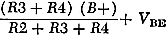
or approximately 5.5 + 0.6 = 6.1 volts. A positive pulse can be obtained
by dividing R2 into two separate resistors and taking the output between them.
In summary then, we have shown that it is possible to simulate the characteristics
of four-layer diodes, SCR's, and UJTs by simply wiring together a pair of transistors
and some resistors.
Posted July 3, 2017
|