|
February 1971 Popular Electronics
 Table of Contents Table of Contents
Wax nostalgic about and learn from the history of early electronics. See articles
from
Popular Electronics,
published October 1954 - April 1985. All copyrights are hereby acknowledged.
|
Other than for DC
power supply applications where you might need to implement current steering
and/or redundancy schemes, there are not too many times when a combination of
transistors and/or diodes would be used for logic circuitry in place of
integrated circuits. That has not always been the case. Early packaged IC blocks
were expensive compared to discrete components, so both hobbyists and
professional designers often used a combination of technologies.
Resistor-transistor logic (RTL) and diode-transistor logic (DTL),
emitter-coupled, logic (ECL), and other variations were covered in a 1969
Radio-Electronics article by titled "How IC's Work: Integrated Circuit Logic Families."
This piece provides a little more insight into the construction of those
families and shows how to construct logical combinations using diodes and NOR
gates. As noted in my Radio-Electronics write-up, the Apollo
Guidance Computer used only 3-input NOR gates to build RTL circuits for all of
its solid state logic capability.
Discrete Components Yield Better Understanding
Part 1 of a 2-Part Story by Frank H. Tooker
Virtually all RTL (resistor-transistor-logic) integrated circuits can be duplicated
from conventional discrete components. This enables the builder to design and test
circuits at the same time - well before an IC is selected and installed. Various
logic gates, latch circuits, and half-adders are discussed in this part of the article.
The integrated circuit has been with us for barely a decade and in use in hobbyist
and experimenter circles for roughly half that time. Yet, the IC has had a profound
effect on every area of electronics, making possible the present sophistication
of modern digital equipment.
The digital computer, for example, is often viewed erroneously as a complex device
of gigantic proportions. But you have only to consider how much more complex and
larger in size it would have to be if it were assembled entirely with discrete components.
Without the IC, a digital computer could easily occupy the volume of a small house.
What is true of the digital computer is also true of all digital logic devices,
including communication, telemetry, and instrumentation systems, as well as the
digital test equipment many home enthusiasts use on their workbenches. Without integrated
circuits to simplify and miniaturize electronic devices, our space program would
still be where it was ten years ago, information processing would be slow and tedious,
and it is more than likely that digital test equipment would never have evolved.
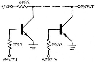
Fig. 1 - N-input integrated circuit gate.
The purpose of this article is to provide information needed to breadboard IC
logic element equivalents, or near equivalents. "Equivalent" - as used here - refers
to the function and not the configuration of the IC and discrete circuits.
In this first of a two-part story on resistor-transistor logic (RTL), attention
is focused on logic gates. (The glossary explains the distinction between the three
fundamental types of digital logic systems - RTL, DTL, and TTL - and provides definitions
for the various technical terms used in this article.) Installment number two will
deal with the more sophisticated toggled logic circuits, including the JK flip-flop.
Virtually every RTL element consists of some form of logic gate which operates
in much the same manner as a common relay. The gate requires an input activating
force and a two-state (on/off, high/low, or logic 1/logic 0) output. Only two output
states arc necessary for digital circuits to communicate in their two-digit, or
binary arithmetic, language. Consequently, the basic elements of digital systems
are quite simple.
Compared to the 0-to-9 decimal system of arithmetic, however, binary arithmetic
requires a tedious number of operations to perform the same function and process
the same information. The extra operations, of course, require extra logic elements
which, in turn, give all digital equipment the appearance of being complex.
The actual simplicity of a digital logic element can be seen in the two-input
IC logic gate shown in Fig. 1. If only one stage of this circuit is considered,
it is the configuration of an inverter, or one-input gate, in an integrated circuit.
This gate could not be simpler, consisting of a single transistor and its associated
base resistor. A hex-inverter IC would contain 6 such inverters, all connected to
the power source through a common 640-ohm collector load resistor. (Note: Integrated
circuit designers have chosen 450 ohms and 640 ohms for the base and collector load
resistors, respectively. These values give the circuit optimum fan-in and fan-out.
The 450- and 640- ohm values used inside IC's are not commonly available in discrete
component form; when you breadboard your elements, you would use 470- and 680-ohm
resistors. These will work adequately.)
The transistors in all RTL integrated circuits are silicon NPN types with characteristics
similar to discrete computer-type switching transistors. All RTL IC's operate from
a power source of 3.6 volts within a maximum tolerance of ten percent.
When breadboarding any RTL element, keep in mind that a computer-type transistor
need not have a linear transfer characteristic since it is never operated in a linear
fashion. It is either completely cut off or fully saturated. However, it must have
certain other characteristics: excellent high-frequency response; comparatively
high saturation current gain; and 0.2 volt or less collector-to-emitter saturation
potential. The latter is important because when the output of one gate is connected
directly to the input of another gate, the output potential of the first transistor,
when saturated, is sufficiently near ground potential to insure that the second
transistor is fully cutoff.
A one-input gate is most commonly referred to as an inverter because its output
is 180° out of phase with its input. In terms of positive computer logic, when
the input is at a logic 1, the output is at a logic 0, and vice versa (logic 1 is
the complement of logic 0). In terms of negative computer logic, the 0's and 1's
change places for the on or off state of a given transistor.
It is simpler to follow positive computer logic where a logic 0 is equal to ground
or near ground potential because the logic designation coincides with the signal
level. As far as logic is concerned, however, it makes no difference whether logic
0 is represented by a near-ground potential or by some potential significantly removed
from ground. If you think of a logic 0 as represented by a cut off transistor, and
a logic 1 as represented by a saturated transistor, then negative logic can be followed
as easily as can positive logic.
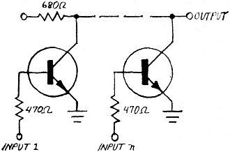
Fig. 2 - N-input discrete-component logic gate.
The schematic diagram of Fig. 1 shows how simple it is to provide additional
inputs to the logic gate. The collector load resistor remains the same for each
additional input stage. Theoretically, at least, IC designers could go on adding
inputs in this fashion until the total accumulated leakage current became excessive.
In easily available IC's, four inputs - in a quad arrangement - are the most you
can get. Within reasonable limits, adding inputs has no significant effect on the
fan-in and fan-out factors of a gate.
There is nothing mysterious about resistors and transistors on an IC chip. They
function the same as their discrete counterparts. So, you can easily assemble an
inverter, a two-input gate, an n-input gate, etc., using discrete components alone.
(The circuits presented from here on arc designed to operate at speeds up to 100,000
Hz, sufficient for experimental purposes. Digital equipment used in science and
industry, of course, becomes practical only because it can operate at speeds in
the MHz range.)
Figure 2 shows how you can breadboard logic gates with discrete components. Readily
available resistor values are somewhat greater than those conventionally used in
integrated circuits, but they are close enough for the most part - especially if
you do not attempt to work your discrete-component setups close to maximum fan-out.
But when working with critical circuits, you shouldn't load your circuits too heavily
in any case.
Almost any high-speed, computer-type silicon NPN switching transistor can be
used in your circuit setups. A good example of such a transistor is the 2N2475 and
HEP56. If you are in an area where surplus parts stores are located, you might be
able to pick up quite an assortment of silicon switching transistors at bargain
prices.
In the absence of computer-grade transistors, you might try using any high-frequency
silicon NPN transistors you have around. But remember to run the input up to where
the transistor is well into saturation, and check the collector-to-emitter potential
with a meter. If the reading obtained is 0.2 volt or less, chances are you can use
the transistor in digital logic-gate service.
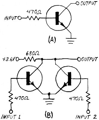
Being able to expand a gate is particularly useful when circuits are being assembled
on your workbench. The circuit in Fig. 3A is an expander, resembling an inverter
or one-input gate with the exception that it has no collector load resistor. Figure
3B shows how all expander can be added to an IC inverter element to make a two-input
logic gate. Simply connect the collector (output) of the expander circuit to the
output of the inverter. The input to the inverter now becomes input 1 and the input
to the expander becomes input 2. Note that the circuit is fundamentally identical
to that in Fig. 1. In a similar manner, you can add all expander to a two-input
gate to create a three-input gate, and so on.

Fig. 3 - Simple expander (A) adds inputs to gate (B).
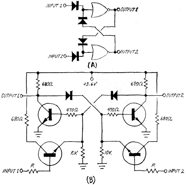
Now, suppose you have a two-input-gate IC, you need a three-input gate, and you
have no suitable transistor on hand to breadboard the expander. You can expand the
two-input gate to a three-input gate by using a couple of germanium diodes as shown
in Fig. 4A. The diodes can be 1N191 or HEP134 types - or any diode with similar
characteristics.
The purpose of the diodes is to keep a logic signal at input 1 from entering
input 2 and vice versa. Yet each diode allows the signal at its respective input
to enter the IC left-gate input. (Note: Discrete and IC configurations can be identified
by whether or not a circle encloses the transistors. Discrete transistors are enclosed
in circles, while IC transistors are not.) If you need a four-input gate, you can
add a similar pair of diodes in the same manner to the input resistor on the second
transistor.
There can be a 0.3-0.4-volt forward voltage drop across each diode, so it is
not advisable to use diode expansion as part of the load in a maximum fan-out configuration.
The transistor expander in Fig. 3A is not subject to this limitation.
On the other hand, if you are breadboarding a two-input gate using a pair of
germanium diodes and a single transistor, as shown in Fig. 4B, you can often get
around the voltage-drop limitation by using a germanium NPN transistor (HEP641 or
similar) in the setup. However, there are significant factors that must be taken
into consideration here. First, germanium transistors can be operated in no more
than a moderate temperature environment since they perform poorly or not at all
at elevated temperatures. (The same, of course, applies to germanium diodes.) Second,
the lower the required logic level, the lower the noise immunity of the circuit.
For those setups where noise pulses or spurious signals are a particular problem,
the circuit in Fig. 4C can be of considerable value. This circuit gates with an
input logic level of 3 volts but is unresponsive to input signals of 1.5 volts or
less. Additionally, its fan-in is only about ten percent that of a gate with a conventional
input.
From now on, logic symbols will be used in many of the schematic diagrams in
this article. The logic symbols, with their equivalent electronic circuits, are
given in Fig. 5.

Fig. 4 - Germanium diodes are often used to add inputs to existing
gates (A) and (B). Typical noise immunity circuit (C) is below.

Fig. 5 - Logic symbols (at left of each circuit) are generally
used in logic flow diagrams.
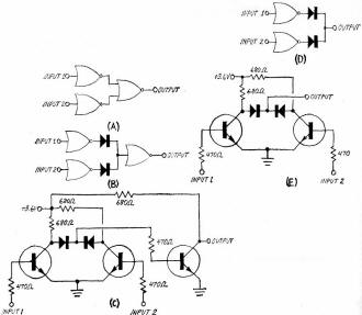
Fig. 6 - Diode pair can be used to make AND gate in (A) from
three inverters as in (B). Discrete-component diagram for (B) is shown in (C); (D)
and (E) are logic and schematic diagrams for NAND gate.
A positive-logic NOR gate is a negative-logic NAND gate. From the point of view
of positive logic, the gates described thus far are all NOR gates in which a logic
1 input to either input 1 or input 2 (or both) produces a logic 0 output.
The circuit in Fig. 6A is a conventional positive-logic two-input AND gate wherein
both inputs must be supplied with a logic 1 signal to generate a logic 1 signal
at the output. This setup requires two inverters and a two-input gate to bring the
input and output signals into phase with each other. The small circles at the apices
of the logic symbols indicate inversion, or a 180° phase displacement, between
the input and output signals. Hence, two gates or inverters are needed to make the
output and input signals of the same phase.
If you have only three inverters and no two-input gate available, you can breadboard
a positive-logic AND gate with the aid of a pair of germanium diodes as shown in
Fig. 6B. An AND gate, assembled with discrete components is given in Fig. 6C.
An AND gate requires two inversions so that logic 1 inputs provide a logic 1
output. Without the second inversion, we would have a NAND gate. In the NAND circuit,
logic 1 inputs provide a logic 0 output. Given in Fig. 6D and in Fig. 6E are the
logic diagram and discrete component schematic diagram for NAND gates.
In comparing the AND and NAND gates, note that a double inversion is equal to
no inversion at all.
In the preceding logic-gate circuits, output logic directly follows input logic.
In the simple two-input gate, for example, a logic 1 at either of the two inputs
produces a logic 0 output. Removal of the logic 1 input by sending the input to
logic 0 produces a logic 1 output.
There are, however, applications where it is desirable to turn on one gate by
applying a signal to one input and turn oft the gate by applying a signal to the
other input. Once such a circuit is energized, it will remain turned on even after
the excitation signal is removed. It will also be unresponsive to succeeding turn-on
signals. Similarly, once it is turned off, it will remain off and be unresponsive
to subsequent turn-off signals. Such a device can be thought of as it "latch" and
is known as an RS (for reset-set) flip-flop.
The fundamental circuit of a latch ran be represented by a pair of inverters,
with the output of one inverter connected directly to the input of the other as
shown in Fig. 7 A. Because inversion occurs in each inverter, it is obvious that
when one side of the circuit is on, the other must be cut off. It is equally obvious
that the on side must remain on and the off side remain off unless something is
done to make the system change states. No provision is made to effect any such control
in the simple circuit shown.
A more practical latch or R.S flip-flop is shown in Fig. 7B. Here a pair of two-input
logic gates is used. One input of each is used for the feedback, and the other is
used for control. A logic 1 signal applied to input 1 sends output 1 to logic 0
and output 2 to logic 1. The circuit then remains in this state - held there by
its own feedback and disregarding any further application or removal of turn-on
signals - until a logic 1 signal is applied to input 2, at which time the output
logic reverses itself.
Only a brief pulse at the proper input terminal is needed to trigger and latch
the circuit in either state. The waveform of the control pulse is not especially
critical. In fact, an RS flip-flop is often used to "shape" a logic pulse by converting
it to a square wave with very steep sides.
If a logic 1 signal is applied to both latch inputs simultaneously, both outputs
will go to logic 0. The final state of the latch will then depend on which of the
two inputs is the last to be removed. Ordinarily, a latch is not operated in this
mode; but if a particular setup calls for such operation, there is no reason why
it cannot be employed.
The circuit in Fig. 7B is given in discrete-component form in Fig. 7C. Depending
on what components you have available, you can breadboard a latch in several different
ways. It can consist of a dual two-input gate IC, a pair of inverters in an IC (plus
a couple of expanders), or four individual transistors if necessary.
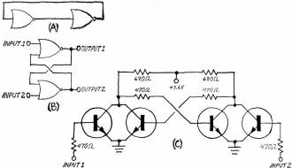
Fig. 7 - Two inverters are employed in fundamental latch circuit
(A). More practical latch is RS ftip-flop illustrated in diagrams in (B) and (C).
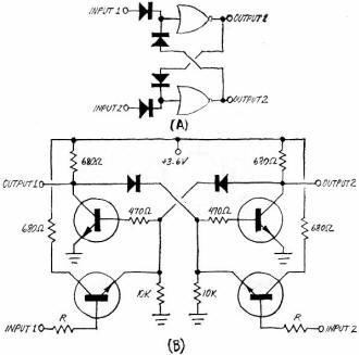
Fig. 8 - Practical latch using inverters is illustrated in diagram
(A); discrete-component circuit for power-gated, or buffered-input, latch is shown
in schematic diagram (B).

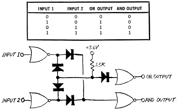
Fig. 9 - Simultaneous AND/OR gate at left employs diodes and
simple inverters. All possible inputs and their outputs are listed in truth table
(above).

Fig. 10 - Simple addition of diode D and resistor R to the simultaneous
AND/OR gate yields the Exclusive OR circuit that is shown at right.
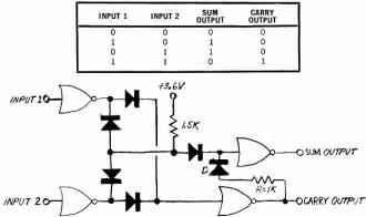
Fig. 11 - Half-adder/subtracter has DIFFERENCE and BORROW outputs
in addition to the SUM and CARRY of Exclusive OR.
If you need a latch circuit and have only a single pair of computer-type silicon
NPN transistors, or a couple of spare inverters in a hex-inverter IC, you can assemble
the fundamental latch circuit in Fig. 7B and gate or trigger it from one state to
the other with germanium diodes. The circuit in Fig. 8A illustrates how this can
be done. It is possible to do this for the same reason that it is possible to use
a pair of diodes for gate expansion, in which the two diodes on each side of the
setup operate as positive-logic OR gates.
In the circuit of Fig. 7B, turn-on of a transistor is accomplished by pulling
its collector down to near ground potential. It then turns on as a result of cross-coupling.
In the circuit of Fig. 8A, the same result is obtained by driving the base positive
with a logic 1 input. Minimum input logic level is about 50 percent higher than
that required by the circuit in Fig. 7B, however.
A power-gated or buffered-input latch circuit is shown in Fig. 8B. A virtue of
this circuit is that, with light loading, it will trigger reliably from one state
to the other with an input current as low as a few microamperes. For a minimum-load
setup, input resistors R can have a value as high as 500,000 ohms. It is important
to note, however, that input logic level must be about 3 volts. Input current is
exchanged for input voltage in this setup. The "high-step" input can help to improve
noise immunity.
You can assemble a power-gated latch using a pair of inverters in a hex-inverter
integrated circuit, or you can breadboard the whole circuit with four transistors
as shown in the schematic diagram. You should use this circuit whenever you have
a sufficient input-logic voltage level but inadequate input-logic current to operate
a more common latch. Do not attempt to get around the higher input logic level requirement
by using a germanium transistor for triggering. Leakage current through a germanium
transistor is too great for this application.
The fan-in of the circuit if Fig. 8B is so low that, when used in the majority
of digital logic layouts, it can be considered as practically an open circuit. It
is especially useful as an exceptionally low-power input start/stop switch in counter
and time-lapse applications.
An element which can supply the OR logic function and the AND logic function
of two inputs simultaneously is of considerable value in digital circuitry. For
one thing, with only slight modification, it forms the foundation for an Exclusive
OR, or Half-Adder, element.
In the simultaneous AND/OR gate of Fig. 9, five diodes and four one-input gates
perform all of the required logic functions. At the output of the two input inverters,
one pair of the diodes provides the AND function, while the other pair, together
with the 1500-ohm resistor, provides the OR function. A logic 1 is obtained at the
OR output when a logic 1 is applied to input 1, input 2, or both inputs simultaneously.
A logic 1 is obtained at the AND output only when a logic 1 is applied to both inputs
simultaneously.
A state table for the circuit is also provided in Fig. 9. This state table lists
all possible in-puts to a digital logic element or device and the outputs which
result from these inputs.
A half-adder or Exclusive OR Logic circuit is shown in Fig. 10. The circuit is
obtained by adding resistor R and diode D to the OR circuit of Fig. 9. (In some
cases the diode may be omitted.)
In the circuit in Fig. 10, the Exclusive OR output is the SUM output, and the
AND output is the CARRY. As shown by the state table in Fig. 10, the circuit provides
a logic 1 at the SUM: output when a logic 1 is supplied to either - but not both
simultaneously - input. When a logic 1 is supplied to input 1 and input 2 simultaneously,
the output is a logic 0, as it is when both inputs are logic 0. The outputs of the
circuit demonstrate the fact that a logic 1 added to a logic 0, or vice versa, produces
a sum of 1 and a carry of 0. A logic 1 added to a logic 1 produces a sum of 0 and
a carry of 1.
A half-adder is required to sum only two logic inputs, whereas a full-adder must
sum two inputs and a carry, for a total of three logic inputs. (A full-adder consists
of two half-adders, plus some additional circuitry. Details of this circuit would
simply digress from the subject of this article. Also, a full-adder would be impractical
to breadboard in any event.)
Now, if we label input 1 with an A and input 2 with a B, then in a half-adder/subtracter
in which B is subtracted from A, the following happens: First, the SUM output is
identical with the DIFFERENCE output, such that the SUM or DIFFERENCE output supplies
the Exclusive A OR B function. Next, the CARRY output supplies the A AND B function.
And, finally, the BORROW output supplies the BAND A-COMPLEMENT function.
The circuit of a half-adder/subtracter, which can be readily breadboarded, is
given in Fig. 11. It consists of five diodes, four inverters, and a dual two-input
gate (or the equivalent in discrete form). This particular setup also supplies the
complement of the SUM or DIFFERENCE output.
As you can see from the preceding, there is little need - or reason - for you
to make a large financial investment in digital IC's if you want to experiment with
and design logic elements and systems. Discrete components, and maybe a few commonly
used gate IC's, will suffice for your breadboarding arrangements. You can select
your IC's from the knowledge you gain through experimenting with discrete component
elements. This is really the best and safest route to go when experimenting with
integrated circuit digital logic techniques.
Glossary of Digital Logic Terms
Adder: Switching circuit that combines binary information to generate the SUM
and CARRY of this information.
AND: This Boolean logic expression is used to identify the logic operation where,
given two or more variables, all must be logic 1 for the result to be a logic 1.
DTL (Diode-Transistor Logic): Logic is performed by diodes with transistors used
only as inverting amplifiers.
Exclusive OR: A logic function whose output is 1 if either of the two input variables
is 1 but whose output is 0 if both inputs are 1 or 0.
Fan-in: A figure denoting the input power required to drive a logic element satisfactorily.
Fan-out: A figure denoting the power output of a logic element with respect to
logic element inputs.
AND Gate: All inputs must have 1-level signals at the input to produce a 1-level
output.
NAND GATE: All inputs must have 1-level signals at the input to produce a 0-level
output.
NOR Gate: Anyone input or more than one input having a 1-level signal will produce
a 0-level output.
OR Gate: Anyone input or more than one input having a 1-level input will produce
a 1-level output.
Half Adder: A switching circuit which combines binary information to generate
the SUM and CARRY. It can accept only the two binary bits to be added.
Inverter: A circuit whose output is always 180° out of phase with its input.
(Also called a NOT circuit.)
Negative Logic: Logic in which the more negative voltage represents the 1-state;
the less negative voltage represents the 0-state.
Noise Immunity: A measure of the sensitivity of a logic circuit to triggering
or reaction to spurious or undesirable electrical signals or noise, largely determined
by the signal swing of the logic.
RTL (Resistor-Transistor Logic): Logic is performed by resistors. Transistors
are used to produce an inverted output.
TTL, T2L (Transistor-Transistor Logic): A logic system evolved from
Diode-Transistor Logic in which the diode cluster is replaced by a multiple-emitter
transistor.
Posted January 22, 2019
|