|
February 1967 Popular Electronics
 Table of Contents
Wax nostalgic about and learn from the history of early electronics. See articles
from
Popular Electronics,
published October 1954 - April 1985. All copyrights are hereby acknowledged.
|
Yesterday was the 71st anniversary
of the announcement of the transistor's invention by Drs. Shockley, Bardeen, and Brattain
at Bell Labs, but it was a Sunday so not as many RF Cafe visitors saw the commemorative
title graphic I used (see it
here). Their transistor
was a current-controlled signal amplifying device as opposed to the field-effect transistor
(FET) which is a voltage-controlled signal amplifying device - as is the vacuum tube.
I never thought about it before, but maybe that had something to do with the electronics
world's hesitancy to adopt the transistor as a replacement for the tube. Early in the
transistor's history, practical applications were limited due to low reliability, low
power handling, low frequency, lack of ruggedness in harsh operating conditions, and
other shortcomings compared to established and much refined vacuum tubes was reason enough
to shun the newfangled technology, but that current-controlled thing could have been
a barrier inhibiting adaptation as significant as any of the aforementioned obstacles.
By the time FETs became widely available for commercial use, the transistor vs. tube
battle was already tipping in favor of the transistor. FETs initially enjoyed a huge
cadre of cheerleaders in the digital circuit realm due to their extremely low power consumption.
One of the most notable uses of FETs in the analog world was as high impedance inputs
to opamps and voltmeters.
Meet Mr. FET ... the Transistor That Thinks it's a Tube
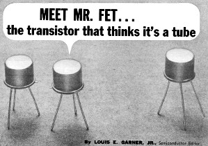 By Louis E. Garner, Jr., Semiconductor Editor By Louis E. Garner, Jr., Semiconductor Editor
This Little Fellow and His Family are Taking over Solid-State
It's hard to imagine, in the light of present scientific and technological achievements,
that just a few short years ago there were no transistors and no integrated circuits.
In fact, there are still many old-timers who remember the "prehistoric" age when there
were no vacuum tubes, either. In those days, radio transmitters were weird spark-sputtering
electromechanical monsters which bore a nostalgic resemblance to the fire-eating dragons
of a yet earlier era.
Radio receivers were simple, too. A huge antenna hooked up to a couple of oversized
coils, a tiny bit of mineral-galena - with a cat's whisker (fine wire), a pair of headphones
... and that was the receiver. The galena, a crystal detector, was cheap, but it was
insensitive and temperamental, too. It was on a quest for a better detector that Prof.
J. A. Fleming developed the diode vacuum tube which, rightly enough, came to be known
as the "Fleming valve."
|

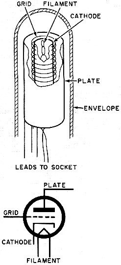
Fig. 1 - Cutaway view illustrates the internal construction of a triode
vacuum tube. The schematic symbol representing this tube is shown below the cutaway view.
|
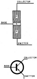
Fig. 2 - Basic junction transistor cross section shows sandwich arrangement
of semiconductor material for pnp unit. Note direction of arrow in the schematic symbol.
|
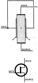
Fig. 3 - Cross section of n-channel junction field-effect transistor
shows p-type regions diffused into n-type substrate. Symbol has not been fully standardized
yet.
|
A short time later Dr. Lee De Forest, inventor and scientist, added the control grid
which, for the first time, enabled the vacuum tube to amplify, oscillate and detect electrical
signals.
With the development of the vacuum tube came a giant industry with a record of spectacular
achievements in radio broadcasting, electronic surveillance, computer technology, and
industrial control. During the course of this industrial revolution, the vacuum tube
was enlarged, miniaturized, modified and refined in many ways, including the addition
of more electrodes. But there was a proverbial fly in the ointment. Most tubes generated
so much heat that they had a relatively short useful life, and this resulted in a high
failure rate for tube-type electronic equipment.
Then, early in 1948, Drs. Shockley, Bardeen, and Brattain - all scientists at the
Bell Telephone Laboratories - announced the invention of a completely new device: a triode
"crystal" which they claimed could amplify as well as detect electrical signals. Dubbed
a Transistor (from TRANsfer and re-SISTOR), the device was nothing more than a tiny cube
of crystalline semiconductor material with two fine wire cat's whiskers. A minute voltage
applied to the base crystal (thereafter called the base) controlled a much larger current
flowing between the two whiskers, one of which was called the emitter, and the other
a collector. The early transistors were expensive, noisy, and not too reliable. But these
disadvantages were offset by their extremely small size, high efficiency and, potentially
at least, manufacturing simplicity.
By 1951, long before this early point-contact transistor posed even a mild threat
to the supremacy of the vacuum tube, a radically new type of transistor, the now common
and widely used junction transistor was introduced.
Of Tubes and Transistors. Although a godsend in many ways, transistors brought a host
of new problems to circuit designers. Essentially a current amplifier, the device could
not be used as a direct replacement for the vacuum tube, which is a voltage amplifier.
It had a low-to-moderate input impedance in contrast to the very high input impedance
of vacuum tubes. In addition, because the transistor has a direct resistive connection
between its input (base) and output (collector) terminals, a multiplicity of circuit
feedback problems had to be solved.
Improved design methods were developed later, and transistorized receivers, amplifiers,
transmitters, hearing aids, toys and industrial controls were produced in vast quantities.
But there were still many circuit requirements where only high-impedance vacuum tubes
could fill the bill, and many designers yearned for a miracle-like device - a transistor
with tube-like characteristics.
As time went by, transistors got better and better. Output voltage and current ratings
were being extended, as were the upper operating frequency limits. But no matter how
the newer transistors were improved, they still had the basic characteristics of earlier
types.
Meanwhile, back at the laboratory, scientists were experimenting with a new solid-state
device, based on a molecular principle described by Lilienfeld as far back as 1928. Shockley,
one of the co-inventors of the original transistor, had proposed a practical transistor-like
device based on Lilienfeld's principle as early as 1948, but it was not until the mid
1950's that a workable device was developed in the laboratories, and practical, reliable
units were not manufactured until the early 1960's.
The new device combined the most desirable features of the versatile vacuum tube and
the efficient transistor. It had high input impedance and offered good isolation between
input and output electrodes. Capable of high gain, it was, at the same time, as small
as conventional transistors and extremely efficient. And, oddly enough, it exhibited
at least one of the important operating characteristics of the vacuum tube - the control
of a current by means of a varying electric field - in a solid-state medium rather than
in a vacuum.
|
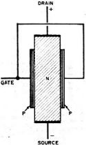
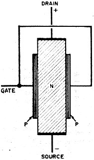
Fig. 4 - Diffusion of p-type regions into n-type substrate provides
a means of controlling the current flow between source and drain electrodes.
|
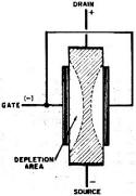
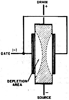
Fig. 5 - When gate is reverse-biased, an electric field is set up
to repel the current carriers, creating a depletion area and restricting region in which
current flows.
|
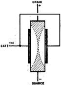
Fig. 6 - As the reverse gate bias is increased, depletion areas spread
into the channel until they meet, creating an almost infinite resistance between source
and drain.
|
Identified by a variety of names - Fieldistor, unipolar transistor, and so on - during
its gestation period, the device is now known as the field-effect transistor (FET). It
is, indeed, a transistor which "thinks" and "acts" like a tube.
Meet Mr. FET. Pictorial and schematic representations of a triode vacuum tube, junction
transistor, and field-effect transistor are illustrated in Figs. 1 through 3. Of the
three schematic symbols, the FET symbol is the least standardized at present.
In a vacuum tube (Fig. 1), the plate current is simply a flow of free electrons which
are literally "boiled" off of the cathode by the heated filament (in some high-power
tubes, the filament is used directly) and are attracted by the positively-biased plate.
The electrons leaving the cathode must travel through the intervening grid.
A negative bias on the grid establishes an electric field which tends to repel the
electrons flowing from cathode to plate, limiting the plate current. The plate current
can also be controlled, within limits, by the plate voltage. However, since the grid
e is much closer to the cathode than the plate, a smaller variation in grid voltage has
essentially the same or greater effect on the plate current as a larger variation in
plate voltage. It is this characteristic that e-ables a vacuum tube to amplify a signal.
Plate current saturation occurs when the plate is attracting all available free electrons.
When this point is reached, a further increase in plate voltage does not cause a corresponding
increase in plate current.
The basic junction transistor (Fig. 2) consists of three sandwich layers of two different
semiconductor materials. Here, the emitter-collector current consists of a movement of
two types of particles: electrons, which are negatively charged, and "holes" (essentially,
the absence of an electron in an otherwise stable crystalline structure) which carry
a positive charge. If the electrons predominate, they are called majority carriers and
the holes minority carriers, with the material identified as an n-type semiconductor.
By the same token, a material in which the positive holes predominate is called a p-type
semiconductor.
The transistor's emitter-collector current is controlled by the injection of minority
carriers into the base region. Since the base is quite thin, a relatively small current
change there can control a much larger emitter-collector current. The junction transistor,
then, is a current amplifying or control device, in contrast to the vacuum tube, which
is essentially a voltage amplifier. In addition, since a base current flow, however minute,
is essential to operation, the device must have a low input impedance.
The basic field-effect transistor consists of a slab of either n- or p-type semiconductor
material with an electrode at either end, and two electrodes along the sides as shown
in Fig. 3. Observe that the side electrodes are tied together and thus function as a
single element. By convention, the terminal into which current is injected is called
the source, and the output terminal is called the drain. The remaining electrode, which
serves as a control element, is called the gate. Notice how FET terminology thus differs
from that of both vacuum tubes and junction transistors.
|
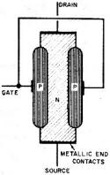
Fig. 7 - A JFET can be manufactured by diffusing p-type gates on either
side of an n-type substrate, and then attaching suitable electrodes.
|

Fig. 8 - This junction FET features single-ended construction. Here,
an n-type channel is formed on one side only of a p-type substrate by photo-masking,
etching, and impurity diffusion processes. The surface is covered with an insulating
oxide layer through which holes are cut for electrode connections.
|

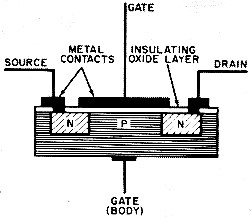
Fig. 9 - Cross-section view of insulated-gate field-effect transistor
(IGFET) shows gate metal contacts insulated by a thin layer of oxide which, together
with the semiconductor channel, forms a capacitor. The metal contacts serve as one plate
while the substrate material serves as other plate of capacitor.
|
How the FET Works. The basic junction FET (JFET) is essentially a bar of doped silicon
that behaves like any ordinary resistor. Refer to Fig. 4 and assume that the FET is made
up of an n-type substrate (material). Then, current through the device will consist principally
of electrons as majority carriers. Consider what happens when a d.c. voltage is applied
to the source and drain electrodes, while the gate is at zero bias. Under these conditions
the device behaves more or less like an ordinary resistor. Within limits, source-drain
current flow is directly proportional to applied voltage.
Now suppose a reverse bias is applied to the gate. (This would be a voltage of the
same polarity as the majority carriers; that is, negative for n-type material, positive
for p-type material.) The gate voltage would then set up an electric field to repel the
current carriers, and restrict the region through which they flow. This action is shown
in Fig. 5. In essence, the current-carrying channel is depleted of current carriers within
areas immediately adjacent to the gate electrode. Logically enough, the regions where
current movement is restricted are termed the depletion areas (sometimes referred to
as zones or regions rather than areas).
A further increase in the reverse gate bias further expands the depletion areas, as
shown in Fig. 6, further reducing drain-to-source current. Thus, with a given fixed gate
bias, the drain current will vary with the signal applied to the gate. Note, also, that
since the gate is reverse-biased, the FET has a very high input impedance when there
is little or no drain current flow. The FET behaves much like a vacuum tube in that drain
current is controlled by an electric field set up by the gate voltage.
Consider what happens when the gate bias is zero and the source-drain voltage is gradually
increased. Up to a point, drain current will increase linearly as in a resistor. However,
the drain current flowing along the channel sets up an internal reverse bias along the
surface of the gate. This, in turn, establishes an electric field which causes a gradual
increase in the depletion areas similar to the effect produced by the application of
an external gate bias. Eventually, the increase in the depletion areas, which tends to
limit drain current, reaches the point where it counterbalances the drain current increase.
From then on, there can be no further increase in drain current regardless of any further
increase in drain-source voltage.
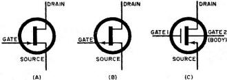
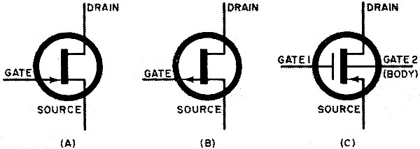
Fig. 10 - Schematic symbols currently used for field-effect transistors
include (a) n-channel JFET, (b) p-channel JFET, and (c) one form of p-channel IGFET.

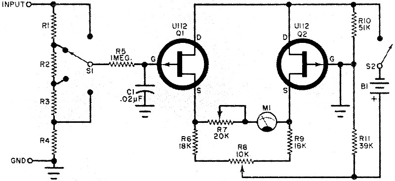
Fig. 11 - This FET voltmeter, featuring a matched pair of Siliconix
U112 FET's in a differential amplifier arrangement, has a sensitivity of 0.5 - 1.0 volt
full scale.
In effect, the drain current has reached saturation (that should be a familiar term!).
The point at which this current limiting takes place is called the drain-source pinch-off
voltage. And there is, as you might suspect, a pinch-off voltage for any given gate bias.
With higher gate bias voltages, pinch-off occurs at much lower drain currents, of course.
If drain current is plotted against drain-source voltage for a given gate bias, a
FET characteristic curve is developed. A family of such curves may be prepared by plotting
drain-source current vs. drain-source voltage for a number of different gate bias voltages.
When compared to corresponding families of vacuum tube characteristic curves, the typical
FET is found to have characteristics which are virtually identical to those of a pentode
vacuum tube.
The FET Family. Field-effect transistors are manufactured using techniques that are
almost identical to those used in the manufacture of the familiar junction transistor.
For example, a FET can be assembled by diffusing or alloying p-type gates on either side
of an n-type substrate and then attaching suitable metallic electrodes, giving the appearance
of Fig. 7.
From a production standpoint, it is often easier to carry out all diffusion and processing
operations from one side of the substrate. This type of single-ended construction is
illustrated in Fig. 8. Manufacture starts with a wafer of p-type material. Photo-masking,
etching, and impurity diffusion processes form an n-type channel on one side of the material.
A p-type gate is then diffused into the n-type channel, and the entire surface is covered
with an insulating protective oxide layer, with holes etched through the oxide for the
final metallic electrode connections.
If you have been wearing your "thinking cap," you may be wondering, at this point,
just why the gate electrode is joined electrically to the channel material. After all,
the gate is reverse-biased in use, causing the p-n junction to behave as if it were a
dielectric. Furthermore, the operation of the device is based on the presence of a varying
electric field on the gate and not upon the movement of current carriers from the gate
to the channel region.
So, why not insulate the gate? Good question, but someone else thought of it before.
As a matter of fact, insulated-gate FET's (IGFET's) are actually being produced by several
major manufacturers. One type of construction is illustrated in Fig. 9. Here, the gate
is insulated by a thin layer of oxide. The gate metal area is overlayed on the oxide
and in conjunction with the insulating oxide layer and the semiconductor channel forms
a capacitor. The metal area serves as the top plate of the capacitor, while the substrate
material is the bottom plate.
In some cases, the IGFET's are assembled as tetrode devices, with the substrate body
(often identified as gate 2) connected to a separate electrode. Since the drain and source
are isolated from the substrate, any drain-to-source current in the absence of gate voltage
is extremely low because, electrically, the structure is equivalent to two diodes connected
back to back.
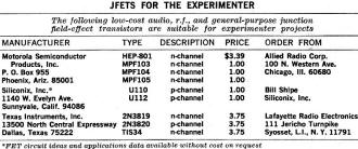
Table 1 - JFETs for the Experimenter
Insulated-gate FET's have extremely high input impedances - higher, in fact, than
many vacuum tubes - but are very sensitive to stray electrical charges and can't be destroyed
by body static. Input impedances higher than 10 million megohms are not uncommon. Manufacturers
generally wrap IGFET leads in metallic foil, or supply them with the leads held together
by a metal eyelet as a protective measure. Extra care must be taken during installation,
wiring, and testing of the IGFET to prevent its destruction.
The junction field-effect transistor (JFET) shown in Figs. 7 and 8 can be made as
an n-channel or a p-channel device. As with conventional junction transistors, JFET's
are identified by the slightly modified schematic symbols shown in Figs. 10(a) and 10(b).
With the source considered common, an n-channel FET requires a positive drain voltage
and a negative gate bias; the p-channel FET is operated with a negative drain voltage
and a positive gate bias.
As shown in Fig.10(c), the IGFET is identified by an entirely different symbol. This
general type of FET is offered in two basic forms and in many individual types with different
electrical specifications and operating characteristics. Unlike the JFET, however, a
given IGFET may require either a positive or negative gate bias, with respect to its
source, depending on mode of operation.
In addition to regular FET's, light-sensitive FET's are being produced by a number
of manufacturers. Called photoFET's, they are similar to conventional FET's but are equipped
with transparent lenses that focus external light on their sensitive surface areas. The
photoFET can be up to ten times as sensitive as a junction phototransistor, and has a
better gain bandwidth factor, in addition to offering exceptional isolation between input
and output circuitry.
Terminology. As with any new technology, a number of terms are used to describe FET
devices, and their characteristics. Some terms are used primarily by manufacturers, others
chiefly by circuit designers. Unfortunately, the terms and symbols have not yet been
fully standardized, with the result that different manufacturers may use different terms
and symbols to represent the same thing.
During its early developmental stages, the FET was identified by different names.
At various times it has been called a Fieldistor, UNIFET, and Unipolar field-effect transistor.
The UNIFET and Unipolar terms were derived from the single-junction construction of the
FET as contrasted to the two-junction (or bipolar) construction of the junction transistor.
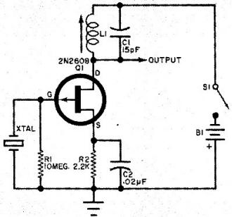
Fig. 12. This high-frequency crystal-controlled oscillator employing
a Siliconix 2N2608 p-channel FET has a useful operating range of 1 megahertz.
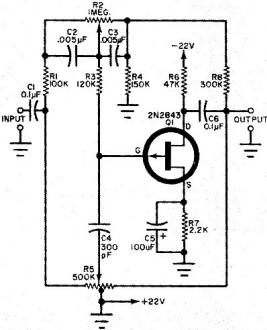
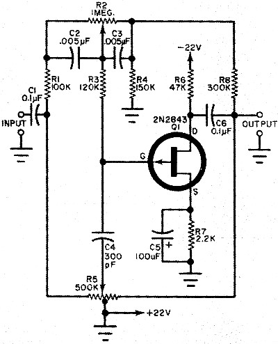
Fig. 13. Modified Baxandall hi-fi tone control employs a single p-channel
FET (Siliconix 2N2843). Separate bass and treble controls are provided.
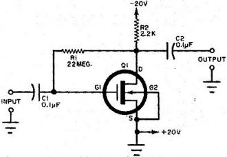
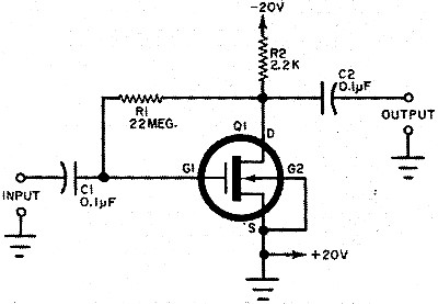
Fig. 14. Definitely not recommended for the experimenter, this single-stage
preamplifier features an insulated-gate field-effect transistor (IGFET).
The name Fieldistor is practically ob-solete today. And so are the other names, although
one firm still refers to its products as UNIFETS. Generally, junction-type units are
simply referred to as FET's, although some firms use the more specific designation JFET.
Insulated-gate field-effect transistors are also called MOSFET's in recognition of
the importance of the metal-oxide-semiconductor (MaS) insulating film used in their construction.
But some de-signers refer to the same device simply as MOST. The latter could lead to
an expression such as "Gosh, Mr. FET, you're the MOST."
At times, the full expressions used to identify a specific transistor may assume an
awe-inspiring length. For example, a data sheet from one firm identifies a specific unit
as a - hold your breath - low-noise, n-channel epitaxial planar silicon tetrode field-effect
transistor!
In addition, not all manufacturers describe their products using the same specifications.
A parameter which is considered important by one company may be completely ignored by
another. As a general rule, however, the majority of manufacturers do give maximum voltage
ratings, input and output capacitances, maximum power dissipation, and typical gate cutoff
current. Many even specify the common source forward transconductance (in μmhos, as
in tube specifications) for typical operating conditions.
Naturally, references are still made to n-channel or p-channel types, as well as to
enhancement or depletion modes of operation. The fact that both n- and p-channel types
are available permits FET's to be used in a variety of complementary circuits, a characteristic
that FET's do not share with vacuum tubes.
Some firms, in striving to simplify matters, have adapted type designations to indicate
the intended mode of operation of the device. Thus, Type A FET's are characterized for
depletion-mode operation; Type B are intended for either depletion or enhancement modes;
and, finally, the Type C designation is reserved strictly for enhancement-mode types.
But please don't confuse these designations with Class A, B or C amplifiers!
Typical FET Applications. With high input and output impedances and other tube-like
operating characteristics, FET's may be considered as almost the solid-state equivalents
of vacuum tubes, and can be used in virtually identical circuits, provided power ratings
are observed. The common source configuration is the most popular, and corresponds to
the common-cathode tube circuit arrangement. Typical FET circuits are illustrated in
Figs. 11 through 14.
Figure 11 is a FET voltmeter with a matched pair of p-channel FET's (Q1 and Q2) used
in a differential amplifier arrangement. In general, FET voltmeters compare favorably
with good-quality VTVM's.
A high-frequency crystal-controlled oscillator employing a p-channel FET is shown
in Fig. 12. .Gate bias is provided, as in a vacuum tube circuit, by source resistor R2,
bypassed by C2. The feedback needed to start and sustain oscillation is furnished by
the FET's inter-electrode capacity as well as by stray wiring capacities.
Figure 13 features a single p-channel FET, Q1, in a modified Baxandall hi-fi tone
control circuit which can be used as part of a stereo control center. Potentiometer R2
serves as the bass control, and R5 as the treble control.
Finally, a simple preamp circuit using an IGFET (MOSFET, or MOST, take your choice)
is given in Fig. 14. Here, gate bias is provided by a 22-megohm resistor, R1, returned
to the drain electrode.
These circuits illustrate a few of the many practical applications of the FET. They
are not intended for use in construction projects as shown, since some component values
might have to be changed to compensate for the use of different FET's. In any case, only
an experienced technician should attempt to use an IGFET in the application shown in
Fig. 14. Practical FET projects will be covered in future issues.
One thing is certain: Mr. FET is a real "comer," and should have a brilliant future!
Posted December 14, 2018
|