|
March 1963 Popular Electronics
 Table
of Contents Table
of Contents
Wax nostalgic about and learn from the history of early electronics. See articles
from
Popular Electronics,
published October 1954 - April 1985. All copyrights are hereby acknowledged.
|
Mr. Einstein believed everything
is relative, and this 1963 Popular Electronics magazine article on the
revolution of "microminiature electronics" certainly attests to the truth of it.
Unlike with his Theory of Special Relativity though, travel near the speed of light
is not needed to witness length contraction in the electronics realm; the passage
of time and its attendant evolution of technology does that for us. Today's definition
of "microelectronics" will to our progeny seem laughingly absurd when they read
about (or more likely have wirelessly implanted in their brain's memory cells) our
current transistor gate widths of tens of atoms.
BTW, Lilliput, in case you don't know, is the island nation of
Gulliver's Travels where the
wee Lilliputians famously lashed Lemuel Gulliver to the beach in his sleep after
washing ashore following a shipwreck.
Littler Than Lilliput: Microminiature Electronics
 By Louis E. Garner By Louis E. Garner
The story of the microminiature in today's electronics
The scene is a radio-TV service shop of the future. The technician wears white
coveralls, a tight-fitting headpiece, thin gloves, and special covers for his shoes.
He works in an atmosphere that is dust- and lint-free, temperature-controlled, and
air-conditioned. His "workbench" is a vacuum-box equipped with tweezer-type micro-manipulators,
a binocular microscope, and an electron-beam welder/etcher. Missing are such present-day
tools as long-nose pliers, diagonal cutters, and a soldering iron. Missing, too,
are stocks of individual components - such as resistors, capacitors, coils, diodes,
and transistors. Instead, the technician tests and replaces complete multi-stage
elements so small that an entire receiver circuit scarcely covers a dime.
Impossible? Not at all. In fact, prototypes of this future "service shop" are
already in use in the research and development laboratories of several manufacturers
- staffed by engineer/technicians who inspect, test, and modify circuits which are
no larger than the head of a pin.
For decades, science-fiction writers and comic-strip artists have envisioned
all sorts of ultra-miniature electronic equipment. Among these items have been rocket
navigational systems and computers no bigger than cigar boxes, tiny "spy" television
cameras concealed in cigarette cases, and vest-pocket-sized two-way radios.
As is often the case, however, science has a way of overtaking and surpassing
its prophets. If current progress in miniaturization is any criteria, even Dick
Tracy's two-way wrist radio will turn out to be "oversized." The reason: it may
one day be possible to assemble a two-way radio in an ordinary finger ring!

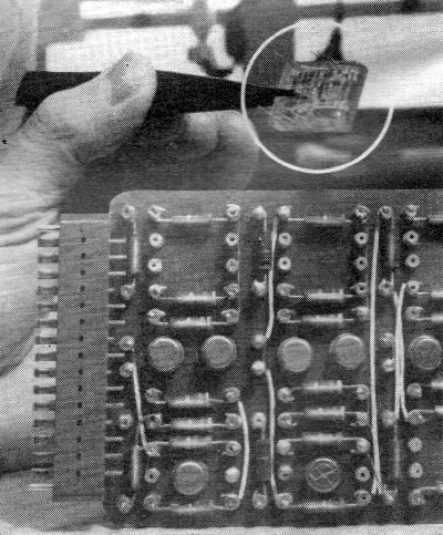
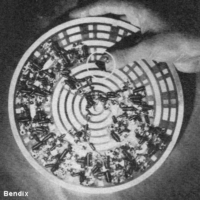
Microminiature electronic module (in circle) performs same functions
as circuit board below it, also employs 35 components, yet is 1/47th the size!
Evolution. Before examining the current situation, let's turn
back the pages of history. The trend towards circuit miniaturization began long
before World War II. It was evidenced, in part, by the introduction of "miniature"
vacuum tubes for conventional applications and "subminiature" tubes for compact
equipment, such as hearing aids. Quite understandably, this trend was given tremendous
impetus during the war. The result was development of a hand-held transceiver (the
handie-talkie) and the now-famous proximity fuse - a transceiver so small that it
could nestle with-in the nose of a bomb or an artillery shell.
For nearly two decades, progress towards equipment miniaturization followed a
gradual, or evolutionary, rather than revolutionary, path. Component parts were
made smaller and circuits more or less "squeezed" together into tinier packages.
But the components still resembled their full-sized counterparts, and conventional
wiring techniques were employed.
A giant step forward came with the invention of the transistor. This device and
its related semiconductor "cousins" - coupled with etched wiring and tiny low-voltage,
low-power components - permitted the production of subminiature circuits. And the
results have been truly fantastic.
A little over a decade ago, for example, the common hearing aid was about the
size of a pack of cigarettes and weighed several ounces. But today's transistorized
hearing aid weighs only a small fraction of an ounce and occupies about one-fifth
of a cubic inch!
Today, two factors have made further miniaturization a prime goal One is the
increasing complexity of electronic equipment - a typical computer uses tens of
thousands of components and may well fill a small room, even when transistorized
and assembled with conventional subminiature components.
 The second factor is the increasing
need for a very short signal response time, particularly in computers and high-frequency
radio circuits. Regardless of the speed at which individual circuits are made to
function, a certain amount of time is required for a signal to travel from one part
of the equipment to another. As a general rule, if the equipment is made smaller,
physically, the signal path is reduced and the operation made speedier. The second factor is the increasing
need for a very short signal response time, particularly in computers and high-frequency
radio circuits. Regardless of the speed at which individual circuits are made to
function, a certain amount of time is required for a signal to travel from one part
of the equipment to another. As a general rule, if the equipment is made smaller,
physically, the signal path is reduced and the operation made speedier.
Revolution. An unprecedented effort at further circuit miniaturization
is now being made by a number of manufacturers. The problem is being attacked on
three broad fronts: (a) the use of thin films; (b) the production of microcircuits;
and (c) the development of solid-state circuits. The final aim is the large-scale
commercial production of low-cost, extremely reliable circuits are microscopic in
size (hence, microminiaturization).
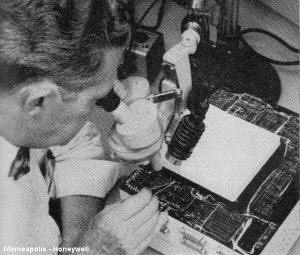
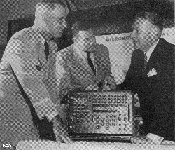
Space and military applications claim the bulk of current "microminiature"
production. New general-purpose digital computer (shown undergoing visual inspection)
was designed for inertial guidance systems.
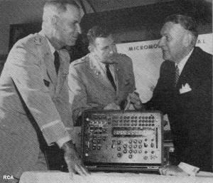
"Micropac" contains nearly 2000 micromodules, will be used by
U.S. Army Signal Corps.

A PRSG (pseudo-random sequence generator) which makes 300 million
"logic decisions" each second.
To this end, the concept of circuit integration has been adopted by most firms.
In essence, an integrated circuit is simply one in which the various elements are
manufactured and interconnected as a unit - there are no separate resistors, capacitors,
coils, and wiring as such. This in itself is a revolutionary concept, since past
efforts at miniaturization generally have been based on the use of individual components.
The key phrase in these efforts is component density, i.e., the number of individual
circuit elements which can be packaged within a cubic foot (or a cubic inch). Not
too long ago, in the days of the subminiature tube, a density of 6000 components
per cubic foot was considered pretty good. With the invention of the transistor,
maximum component density rose to about 100,000 elements per cubic foot. But even
newer techniques promise densities on the order of 10,000,000 parts per cubic foot!
Thin-Film Circuits. Many scientists and engineers consider the
use of thin films as the first true approach to genuine integrated circuitry, since
this technique permits almost all circuit components and wiring to be formed as
a direct part of the manufacturing process. As the name implies, a thin-film circuit
is one made up of ultra-thin metallic films deposited on an insulating base called
the substrate. These films, which can be comprised of such metals as gold, aluminum,
and tantalum, are unbelievably thin - actually one-hundredth as thick as the finest
rolled or beaten foil.
Any of several techniques can be used in forming the thin film, but the three
most popular are electroplating, evaporation, and sputtering. Of these three, electroplating
is quite similar to the methods used in more conventional work except for scale.
Currently, the most popular technique is evaporation. Here, the raw material is
heated to the boiling point in a crucible placed within a high vacuum chamber. The
heated material boils off and condenses on the substrate suspended above the crucible
in the same chamber. Unfortunately, some metals are difficult to evaporate, and
it is with these materials that the sputtering process is employed. In sputtering,
atoms of the metal are splashed onto the substrate by bombard-ing the raw
material with gas ions accelerated by a strong electric field.
Regardless of the basic film forming process used, the circuit elements and interconnections
are produced by arranging the film(s) in a precise pattern. Often, several film
layers are employed, each in a different pattern, to produce resistors, capacitors,
and circuit wiring. The circuit patterns can be developed by a photoengraving and
etching process, applied to a continuous film. Or they can be formed during the
original film deposition by interposing a "mask" between the substrate and source
of metallic atoms. The latter process is roughly analogous to the use of a stencil
for printing.
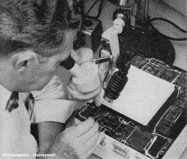
Testing microelectronic circuit materials is a highly exacting science in itself.
Above, scientist wearing special glasses monitors preparation of silicon base material
for a microcircuit. At right, researcher subjects thin-film semiconductors to air
pressure only one-millionth that at sea level.
Production of a typical thin-film circuit begins with thin tantalum and gold
films applied to the insulating substrate (glass in this case). Next, the basic
circuit pattern is formed by photoengraving and etching techniques, using suitable
masks. With the basic circuit pattern established, passive components (such as resistors
and capacitors) are formed by selective oxidation and anodization of parts of the
metallic film. In the last steps, active elements (such as diodes and transistors)
are inserted and final connections made through the evaporation of aluminum electrodes.
As a rule, scores (or even hundreds) of circuits will be processed at the same time.
Generally speaking, thin-film techniques have been suitable only for the deposition
of circuit wiring and the production of passive components ... resistors, capacitors,
and coils. This means that it's been necessary to produce the active elements (diodes,
tunnel diodes, transistors, etc.) separately and then insert these units in the
basic assembly during the last production steps. This process is a costly one, of
course, and - several firms are striving to develop practical methods which will
permit the formation of active as well as passive components with thin-film methods.

Micro-Circuits. Another popular technique for manufacturing
microminiature circuits is based on the use of conventional transistor assembly
methods. The active "heart" of a modern small-signal diode or transistor is a tiny
chip of semiconductor material about the size of a pinhead - and thus extremely
small compared with the header and case in which it's mounted. This fact first led
a number of semiconductor manufacturers to assemble several transistors and/or diodes
in a single standard-sized case, providing additional contact leads for the extra
units.
Later, several firms started interconnecting the various elements to form such
basic circuits as direct-coupled amplifiers, diode matrices, complementary amplifiers,
flip-flop's, Darlington stages, and choppers. Externally, the completed circuit
assembly is the size and shape of a conventional transistor package, except for
the additional leads involved.

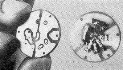
Circuit wafer for diode commutator contains 16 diodes and four
resistors, easily rests on finger tip.

Tunnel diode transistor modules for new computer employ subminiature
versions of standard parts.
While integrated and ultraminiature by definition, micro-circuits assembled on
standard headers from individual diodes and transistors are not as representative
of a new manufacturing process as they are of a refinement in assembly techniques.
The circuit designs employed generally depend on direct coupling between semiconductor
devices, with a minimum of external components (such as resistors and capacitors).
The use of micro-circuit assemblies has made possible a considerable increase in
component density, however, with a corresponding decrease in overall equipment size.
Price-wise, micro-circuits provide an excellent example of what we can expect
as production techniques are refined and as the economies of mass production come
into full play. When first introduced, these units sold for over one hundred dollars
each, even in modest quantities. Today, some firms offer complete circuit assemblies
in several standard configurations at prices approximating those of some transistors!
Solid-State Circuits. Thin-film techniques and micro-circuit
assembly methods have accomplished miracles in miniaturization and offer tremendous
promise for the future. But perhaps the ultimate approach to microminiaturization
is the production of a complete circuit as a single semiconductor device - in essence,
a solid crystal which performs the same function as a conventional circuit through
a rearrangement of its internal molecular structure, and without the need for individual
active and passive electrical elements.
When perfected, this technique may permit the manufacture of a pinhead-sized
crystal capable of performing all the functions of an amplifier or oscillator stage.
Interconnected, a few such "pin-heads" could serve as a complete receiver or amplifier.
One manufacturer, for example, is now developing a computer using solid-state circuits.
The completed instrument will weigh less than 15 pounds and occupy less than one-third
of a cubic foot, compared with the 175-pound weight and three-cubic-foot space requirements
of an equivalent "miniature" transistorized computer.
The basic steps in the fabrication of at least one type of solid-state circuit
are essentially similar to the methods used for the production of individual diodes
and transistors (see "Transistors - Types and Techniques," Popular Electronics,
November, 1962, p. 64). The base material on which the circuit is formed is a wafer
of semiconductor material (such as silicon) rather than an insulating substrate.
Area masking, photoengraving, etching, and impurity diffusion techniques are
used to form appropriate p- and n-type semiconductor regions in the wafer to produce
various circuit elements. Evaporation methods are then employed to apply metallic
conductors. And, finally, the wafer is mounted in a suitable case (such as a ceramic
wafer), the crystal is diced to isolate individual elements, and circuit interconnections
are made.
Summing Up. At present, the majority of commercially available
thin-film, "micro-circuit," and solid-state microminiature circuits are used in
computer designs ... flip-flop's, gates, buffer amplifiers, shift registers, adders,
and memory arrays. There is a good reason for this - of all electronic systems,
computers require the greatest number of repetitive circuits, and it is here that
the advantages of the multiple production of identical circuits can be utilized
to the fullest extent.
As far as consumer products are concerned, microminiaturization of circuitry
will offer few advantages until "accessory" components (microphones, speakers, etc.)
can be subjected to a similar "shrinking" process. Research is being conducted along
these lines, however, and there is a definite possibility that micro-miniaturization
will be applied to such units as hearing aids, walkie-talkies, personal receivers,
amplifiers, and similar products in the not-too-distant future.
As for industrial applications, one firm has confidently estimated that the market
for microminiature circuits will approach twenty billion dollars a year by 1980!
Posted December 20, 2021
(updated from original post on 5/30/2014)
|