|
September 1972 Popular Electronics
 Table of Contents Table of Contents
Wax nostalgic about and learn from the history of early electronics. See articles
from
Popular Electronics,
published October 1954 - April 1985. All copyrights are hereby acknowledged.
|
People are entering
the field of electronics all the time and many want to learn not only circuit theory
and troubleshooting, but design as well. With all the pre-packaged integrated circuits
available that perform just about every function imaginable, there are still times
when you either want or need to set about designing your own circuit. Interfaces
between two circuits, or to displays and sensors are examples of the kinds of applications
that might need a custom design. That applies not only for RF type circuits that
require impedance matching, but also to low frequency analog and digital circuits.
This article by Mr. Jim Huffman, which appeared in a 1972 issue of Popular
Electronics, provides an introduction on how to methodically determine all
necessary requirements and then actually design your circuit - in this case an audio
amplifier. A technician I worked with in the early-to-mid 1980s who was an inspector
at Westinghouse Oceanic Division, in Annapolis, Maryland, designed a battery-powered,
pocket-sized amplifier for driving a set of headphones from his electric guitar.
It was his first "real" circuit design and he doted over it like it was his newborn
child. He came up with a great name for it: the "Jam Anywhere."
Simple Solid-State Circuits for the Experimenter
Basic Approach Enables Anyone to "Roll His Own" Amplifier
By Jim Huffman
You don't have to be a mathematical genius to design a simple solid-state amplifier.
All you have to do is follow some basic rules, cut-and-try a little, test the circuit,
and there it is! The mathematics involved in complete, top-level circuit design
require the knowledge of a graduate engineer; but, unless the circuit is critical,
there are some shortcuts that can be used by the serious electronics experimenter.
These shortcuts yield "ballpark" figures that work well with components having 5%
or 10% tolerances.
To explain what we mean by shortcuts and simplicity, we will use as an example
the design of a microphone preamplifier. In this design, math is at the high school
level, and Ohm's Law is the most complicated formula involved. All the designer
has to do is "plug in" the numbers necessary for his particular application.

Fig. 1 - Write down basic circuit facts.
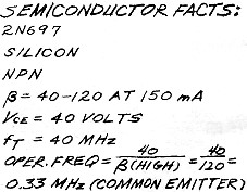
Fig. 2 - Consider transistor characteristics.
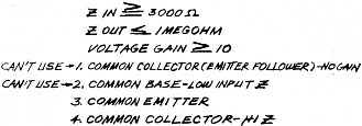
Fig. 3 - These are circuit parameters.
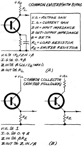
Fig. 4 - Two circuit configurations.
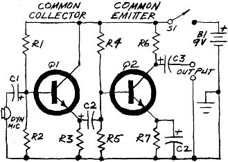
Fig. 5 - Draw basic circuit diagram.

Fig. 6 - Determine the resistor values.

Fig. 7 - Convert to equivalent ac design.
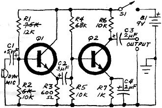
Fig. 8 - This is the final circuit layout.

Fig. 9 - Testing input/output impedances.
Preamplifier Design
Suppose you want a microphone preamplifier that will match a low-impedance dynamic
mike to a modulator or power amplifier with an input impedance of one megohm. (In
other words, you want to make the dynamic mike "100k" like a crystal mike.) Note,
however, that the same procedure described here could be used for matching an input
device of any impedance to any circuit impedance simply by changing the necessary
figures and using the appropriate transistor.
The design is accomplished in eight easy steps:
- Write down all the pertinent facts about the circuit (see Fig. 1). It was determined
(by tests) that the output of a crystal mike hits a maximum of 0.5 volt (roughly
that of a crystal phonograph pick-up). The dynamic mike was connected to a VTVM,
and a no-load output voltage of 0.1 volt was measured when speaking loudly, so a
normal level of 0.05 volt was used. Thus, the voltage gain required of the amplifier
is about 10 (0.5/0.05). Since these are very rough approximations, a final voltage
gain of at least 20 was decided upon.
- Write down all available facts about the transistor. Since we have a 2N697 in
our junk box, we decide to try it (see Fig. 2). The 2N697 is silicon, so it is stable
with temperature. It is an npn and has a beta between 40 and 120 when the current
is 150 mA. Usually, we use the lowest beta figure, but since the 150 mA specified
for the 2N697 is considerably more than we need, we use a beta of 50. Since we are
using a nine-volt supply and the breakdown voltage, VCE, is 40, the device should
be safe. The gam-bandwidth product, fT, for the 2N697 is 40 MHz. Dividing
this value by the highest beta (120) gives a maximum frequency of 330 kHz, when
the device is used in the common-emitter configuration. This is well above the 3-kHz
maximum frequency required.
- Decide on a configuration, using the facts in Fig. 1. The parameters selected
are shown in Fig. 3. The input impedance may be hard to achieve with a common-base
amplifier; and since the voltage gain is more than unity, the common-collector approach
can't be used. The common emitter (Fig. 4A) looks good except that the input impedance
is higher than that normally associated with a common-emitter circuit. So we have
to add another stage (emitter follower) to raise the input impedance (Fig. 4B).
- Now we can draw a preliminary design, such as that shown in Fig. 5. The battery
supply is included, capacitors are marked for polarity, and components are numbered
for reference.
Note that single-battery bias is used. This bias method provides
better results as far as temperature stability and other factors are concerned.
Also, contrary to some beliefs, this is the easiest system to design.
- Calculate the data as shown in Fig. 6, using the data supplied in Fig. 4A for
the common emitter stage and Fig. 4B for the emitter follower. The most critical
parameter for the emitter follower is the output impedance. The latter is approximately
equal to the input impedance divided by beta, or 3000/50. So the output impedance
(or the emitter resistance) should be 60 ohms or more. This is easy to achieve since
the input impedance of the next stage is probably greater than 60 ohms. The actual
emitter resistor is R3, and to avoid as little loss as possible, we choose it to
be ten times the 60 ohms decided on for the emitter resistance. Thus, R3 = 600 ohms
or more. The "or more" tells us which way to go if we have to use other than a 600-ohm
resistor.
For stability, R2 should be about 10 times R3 or 6000 ohms.
The value of R1 depends on the value of bias current chosen. Since the stage
is a voltage amplifier, and since a 9-volt supply is used, there should be about
4 volts across R3 (including a 1-volt drop across the transistor). Thus, the voltage
at the base of the emitter follower should be four volts when there is no input
signal. To achieve this drop across R2, R1 has to be 7500 ohms. For the
common emitter stage, R7 is a non-critical value in most cases and can be "picked
out of the air." If the wrong value is chosen, we will find out later in the design.
A good value to choose for R7 is 1000 ohms. In this stage, as before, R5
is 10 times R7 or 10,000 ohms. The value for R6, which must be chosen before
R4 can be determined, will be approximately equal to the output impedance of the
amplifier. The modulator or power amplifier input is a voltage amplifier because
of the high impedance. Since the output of the preamp is required to be a voltage
generator, the output impedance can be much less than the input impedance of the
modulator or power amplifier. The stage need not transfer maximum power, only maximum
volts, so the impedances need not match. Essentially, the entire output voltage
from the common emitter stage will he felt at the input of the amplifier if the
output impedance is less than about 1/10 of the input impedance of the amplifier.
In fact, 1/100 would be a better figure, so R6 is chosen to be 10,000 ohms. Normally,
at this time, R6 would be considered in regard to the desired voltage gain. A quick
check shows that the 10,000-ohm value provides a gain of over 20. To make
sure that the output of the amplifier is class A (and since Q2 is a current amplifier,)
the bias through R6 is chosen to be half of its maximum value. The maximum current
through R6 will be about 0.73 mA (1-volt drop in the transistor) or about 0.36 mA
at the class A bias point. Resistor R4 is selected to provide the 0.36-mA
bias current. There should be about 0.36 volt across R1 with bias current flowing.
Since this is a small voltage, we must take into account the 0.8-volt drop at the
base-emitter junction of the transistor. Thus the voltage at the base of the transistor
must be 0.8 + 0.36 or 1.16. Resistor R4 is chosen to provide 1.16 volts across R5.
This turns out to be about 68,000 ohms.
- To calculate the ac values, redraw the circuit showing all bypassed resistors
as shorts to ac and the input impedance of the following stage as resistors (Fig.
7). Note that R1 and R2 in parallel form Rin which is in parallel with
Zin of the emitter follower to form the amplifier input impedance Since
the input impedance of the emitter follower is dependent on the input impedance
of the common emitter, we must determine the latter from Fig. 4A. Since Ic
= 0.36 mA and beta is 50, the input impedance is 3600 ohms. The latter is in parallel
with R4 and RS, the bias resistors. The parallel value of R4 and R5 is approximately
8800 ohms, which, in parallel with 3600, comes to about 2560 ohms.
The 2560
ohms is paralleled by the emitter follower's own R3 so the emitter sees about 500
ohms. The emitter follower input impedance becomes 500 times the beta or 25,000
ohms. The input impedance of the entire amplifier is RIN (3600)
in parallel with 25,000 or 3000 ohms, which is what is desired. If the values were
found to yield an overall input impedance which was not 3000 ohms, the components
would have to be adjusted appropriately. The voltage gain of the amplifier
depends on the gain of the common emitter stage, which, from Fig. 4A, is about 140.
Thus the amplifier meets the gain requirement of at least 20. Capacitor
values are chosen so that the response at 100 Hz is -3 dB. So, we lump the impedances
associated with a particular capacitor and solve for an equivalent Xc.
Since the input impedance is 3000 ohms, Xc1 = 3k and C1 is
0.5 μF (Xc = 1/2πfC). Keep in mind that, if you cannot hit this
value, a larger capacitance will only lower the response and probably won't be undesirable.
Bypass capacitor C4 is associated with a 1000-ohm resistor and its value
will he close to 2 μF. Capacitor C3 and the 10,000-ohm output impedance combine
for a value of 0.2 μF; and the reactance of C2 must be 500 ohms so its value
is about 3 μF. Insert all of the above figures into the circuit as shown
in Fig. 8.
- Breadboard the circuit. When substituting resistor values, keep the same ratio
between the values and increase or decrease until you come close to something you
have. For instance, assume you do not have a 7500- or 6000-ohm resistor for R1 or
R2. You know the values can go up, so find the ratio of R1/R2 - which is 1.25. An
increase in both values will merely raise the input impedance, which is not objectionable.
Thus, as shown in Fig. 8, R1 and R2 were changed to 12k and 10k, respectively, since
they were readily available.
If you want to change the value of R3, you
will have to go higher, since lowering its value would lower the 3000-ohm input
impedance. Keep in mind that, in some applications, the impedance may not be allowed
to be different from that calculated. Now we can build the circuit, apply
power and check the voltage levels at the emitters of both transistors. This tells
us whether the bias values are correct. It also tells us whether or not the circuit
will operate. Then we connect it to the other devices (mike and power amplifier)
to see if the whole thing works.
- You may not wish to perform this last step, but if you have an audio generator,
use the hookups shown in Fig. 9 to measure the important parameters of the circuit.
Figure 9A is used to measure input impedance. Adjust R1 until the voltage at the
input is half its maximum value. (The value of R1 should be greater than the estimated
input impedance of the amplifier. Then remove R1 and measure its rotor-to-end resistance.
This value will be approximately the same as the input impedance of the
amplifier. The output impedance is measured in the same way by adjusting
R2 in Fig. 9B. The voltage gain is found by using the circuit in Fig. 9C and dividing
the output by the input. Frequency response is found by adjusting the frequency
until two points are obtained at which the output is 0.707 times the maximum. These
are the upper and lower 3-dB power-loss points.
Now the design is complete. The checks should show any values that need adjusting.
Parts can now be purchased, printed circuit boards can be etched, etc., etc.
Posted November 4, 2019
|