|
June 1974 Popular Electronics
 Table of Contents
Wax nostalgic about and learn from the history of early electronics. See articles
from
Popular Electronics,
published October 1954 - April 1985. All copyrights are hereby acknowledged.
|
Believe it or not, there
are still people out there - engineers and hobbyists - who design circuits using
discrete transistors. Sure, there is a plethora of integrated circuits that combine
multiple functions into a single package that performs often nearly like ideal components,
and for a lot less money than building an equivalent circuit from individual components.
Still, sometimes a lone transistor with a couple biasing resistors will do the job,
and sometimes the designer just wants to do something different. There are also
plenty of instances where you need to find a replacement of a failed transistor
that has similar form, fit, and function. This article from a 1974 issue of
Popular Electronics magazine might be just the aid you need if you have found
yourself in need of selecting a transistor. Of course if your application is for
high frequency, there are parameters to consider other than those presented here,
but it's a good start.
Transistor Selection Guide for Experimenters
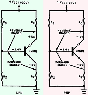
Fig. 1 - Reverse and forward biasing requirements are shown
for npn and pnp transistors.
Understanding transistor circuit characteristics eliminates trial-and-error approach
By Jon L. Turino
Selecting a transistor for a specific circuit application involves considerably
more than just picking a device at random and using trial and error to determine
whether or not it will work. Proper device selection requires that the ratings and
parameters of a transistor be known and that the importance of these characteristics
in the application be understood.
As readers doubtlessly know, the bipolar transistor is normally forward biased
from base to emitter and reverse biased from base to collector (Fig. 1). In
the active mode of operation for the transistor, a small change in base current,
IB, results in a much larger change in collector current, IC.
Transistors also have two other modes of operation - cut off and saturated. In the
cut-off mode, only leakage current flows through the transistor. In the saturated
mode, maximum current flows, limited only by the external components. Even though
we use a transistor primarily in the active mode, we can illustrate many parameters
much more clearly by considering the cut-off and saturated modes.
Parameters and Characteristics. Here are ten transistor characteristics that
should be taken into account when a device is being selected (or when a circuit
is being designed around it). Refer to the proper drawings in Fig. 2 for pictorial
definitions of the parameters.
(1) VCBO: This is the collector-to-base breakdown voltage in the reverse-bias
condition. If the collector-to-base voltage is allowed to exceed the breakdown value,
the transistor may be destroyed. Always select a transistor whose VCBO
rating exceeds the highest voltage expected to exist in the circuit between the
base and collector.
Fig. 2 - Transistor is shown cut off (A), saturated (B),
and in normal mode (C).
(2) VEBO: This is the emitter-to-base breakdown voltage in the reverse-bias
condition. If this value is exceeded, the transistor may be permanently damaged;
so, select a transistor whose VEBO exceeds the maximum voltage that will
exist in the base-to-emitter circuit. (In most "small-signal" analog circuits, the
base-emitter voltage seldom exceeds about 0.8 volt in either the forward or the
reverse directions. Hence, if this parameter is not specified, it will normally
not be cause for concern.)
(3) VCEO: This is the maximum allowable voltage from collector to
emitter with the transistor reverse biased (cut off). The VCEO of the
transistor should exceed the power supply voltage if the transistor is to operate
safely. Alternatively, the supply voltage for the circuit should be maintained at
less than the VCEO.
(4) ICBO: This is the leakage current from collector to base when
the transistor is reverse biased. This parameter is of major importance because
it increases rapidly with increases in transistor temperature. It can affect the
biasing of the transistor stage and, if excessive, cause increasingly large current
flow that can result in "thermal runaway", ultimately leading to destruction of
the transistor. Select a transistor whose ICBO is less than 0.001 times
the normally expected collector current. (Usually, silicon transistors have very
small ICBO ratings. Nevertheless, it is wise to double check.)
(5) VCE(SAT): This is the voltage from collector to emitter when the
transistor is conducting maximum current and further increase in base current will
result in no further increase in collector current. This voltage is the minimum
potential that must be maintained between emitter and collector if transistor action
is to continue. It is usually specified as a specific current, IC(SAT),
and should not exceed the power supply voltage minus the peak-to-peak expected collector
voltage swing.
(6) VBE(SAT): This is the base-to-emitter voltage when the transistor
is saturated. It is usually specified at a specific current, IB(SAT),
and is important primarily in switching circuits, although it does affect the biasing
of analog circuits.
(7) IB(MAX): This is the absolute maximum base current that can safely
flow into the transistor. Care must be taken to insure that the circuit will not
cause base current in excess of IB(MAX) to flow, and, conversely, the
IB(MAX) rating of a device must always exceed the maximum expected base
current.
(8) IC(MAX): This is the absolute maximum collector current that can
safely flow in the transistor. If it is exceeded, the device is likely to destruct.
The IC(MAX) rating should exceed the maximum value of collector current
that can ever flow in the circuit.
(9) P(TOTAL): The total (maximum) power that a transistor can safely
dissipate should never be exceeded. The actual power in a circuit is equal to VCE
X IC when the transistor is biased in the active mode. (The base-emitter
voltage and current also contribute to total power, but they are usually negligible
with respect to VCE X IC.) In most circuits, it is wise to
choose a device whose P(TOTAL). rating is 2 (VCE X IC
).
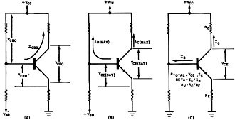
Fig. - 3 This diagram shows how the various parameters are
used in designing a circuit.
(10) HFE This is the current gain of the transistor when in the common-emitter
configuration (shown in Figs. 1-3) and is usually referred to as the transistor's
beta (β). Beta is defined as the ratio of collector current to base current (β
= IC//IB) and is one of the most important of a transistor's
parameters. It determines the achievable circuit gain and the required biasing resistor
values. It might be specified as a range of values (10 to 100) or as a set of values
at specific collector currents (50 @ 1 mA, 20 @ 10 mA, etc.). To select a beta value
for a given transistor, calculate the value of collector current required in the
circuit and the base current available. In any circuit like that shown in Fig. 2C,
beta must exceed the ratio RC/RE but must not be so large
as to allow the transistor to saturate. In a new design, the minimum beta is the
most critical parameter, since the biasing can be tailored for any specific value.
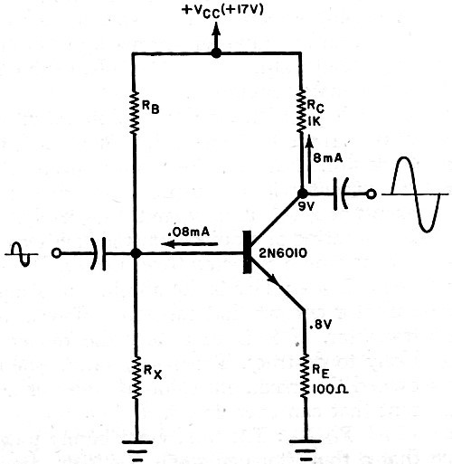
Using The Parameters. The circuit shown in Fig. 3 should help in tying together
all of the seemingly unrelated parameters. With this circuit, we will illustrate
an actual design procedure and demonstrate how each parameter relates to the design.
Let us assume that we need a circuit with a voltage gain of 10 and a peak-to-peak
output swing of 12 volts across a 1000-ohm resistor (RE). We calculate
RE as being 1000/10, or 100 ohms. (Since voltage gain AV =
RC/RE, RE = RC/AV.)
There will be 12 volts peak-to-peak across RC and 1.2 volts p-p across
RE. So that VCE(SAT) does not affect the circuit, add 3 or
4 more volts to the required total potential from the power supply. Make VCC
equal to 12 + 1.2 + 3.8, or 17 volts. With a VCC supply voltage of 17
volts and RC + RE equal to 1100 ohms, the maximum collector
current will be 17 volts/1100 ohms, or 15.45 mA. With the transistor properly biased,
there will be about half of this value (about 8 mA) of collector current. VCE
will be 17 volts - (8 mA X 1100 ohms) = 8.2 volts. Total circuit power, then, is
8.2 volts X 8 mA = 65.6mW.
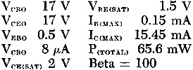 Now specify a value of 100 for the
transistor's beta. At this point, we can select a transistor with the following
minimum characteristic values (right). Now specify a value of 100 for the
transistor's beta. At this point, we can select a transistor with the following
minimum characteristic values (right).
VCE(SAT) and VBE(SAT) are not critical; IB(MAX)
= IC(MAX)/Beta.
 You now have enough information to begin looking through a transistor manual
for an npn transistor with parameter values on the safe side of those listed above.
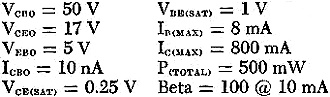
Let us assume that you settle on a 2N6010 transistor with the following characteristics
(left). You now have enough information to begin looking through a transistor manual
for an npn transistor with parameter values on the safe side of those listed above.
Let us assume that you settle on a 2N6010 transistor with the following characteristics
(left).
A comparison of these characteristics with our circuit requirements reveals that
the 2N6010 transistor will more than adequate-ly met our needs. All that is necessary
now is to compute the correct values of RB and RX using conventional
means, and to check out the circuit.
There is a lot of leeway in the selection of a proper transistor for a circuit.
The more conservatively rated the transistor is for a specific application, the
better the probability of the circuit operating almost forever. When it is necessary
to select a replacement transistor, just analyze the circuit for its important parameters
and select a new device whose characteristics fit the requirements.
Posted February 22, 2024
(updated from original post on 5/15/2017)
|