October 1966 QST
 Table
of Contents Table
of Contents
Wax nostalgic about and learn from the history of early electronics. See articles
from
QST, published December 1915 - present (visit ARRL
for info). All copyrights hereby acknowledged.
|
The concept of a field effect transistor
(FET) has been around in theory for a long time*, but manufacturable devices arrived
in designers' labs not until the early 1960s. This article from the October 1966
edition of QST magazine gives a good introduction to the physics of a basic FET
as well as the junction FET (JFET) and the insulated gate FET (IGFET), all of which
are still in widespread use today. What you learn about them here is applicable
today. In fact, I swear some of the drawings are the same ones that appeared in
my college semiconductor physics text books (admittedly from the late 1980s, so
not too much of a surprise).
* Per Wikipedia, "The field-effect transistor was first
patented by Julius Edgar Lilienfeld in 1926 and by Oskar Heil in 1934, but practical
semi-conducting devices (the JFET) were only developed much later after the transistor
effect was observed and explained by the team of William Shockley at Bell Labs in
1947. The MOSFET, which largely superseded the JFET and had a more profound effect
on electronic development, was first proposed by Dawon Kahng in 1960."
Field-Effect Transistors
What They Are-How They Work
By Jim George, W7AWH
The field-effect transistor, for the last few years a tantalizing promise of better
things in semiconductor devices, is now rapidly coming into the market at prices
attractive to amateurs. We've already shown you one application in Walt Lange's
audio oscillator (July QST). Here's the background story of the FET - how it's made
and how it functions, and why it will be superior to older transistor types in many
applications.
A recently introduced semiconductor device called the field-effect transistor,
or FET for short, combines some of the best features of both the vacuum tube and
the transistor. The FET is appearing in new electronic circuits of all types and
will soon be used in amateur radio equipment. A great deal of excitement centers
about this solid-state device which acts much like a vacuum tube, and it is the
purpose of this article to describe its construction and operation.
Before getting into device characteristics, let us quickly review some basic
concepts in semiconductors. Useful semiconductor material is either p-type, where
holes (a hole is actually a place where there is no electron) are concentrated relatively
heavily, or n-type which features an excess of free electrons. Both the holes and
free electrons are the current carriers in a piece of semiconductor, just as free
electrons only are the current carriers in a piece of copper. As a memory aid, remember
that the "p" in p-type material stands for the positive charge of the current carriers
(holes) and the "n" stands for the negative charge of the current carriers (free
electrons) in n-type semiconductor material. When p-type material and n-type material
are brought together, a p-n junction is formed as shown in Fig. 1A.

Fig. 1 - Action of p-n junction when bias is applied.
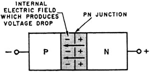
Fig. 2 - Reverse bias causes electrons and holes to move
away from the p-n junction, leaving a depletion region (shaded area) and no current
flows.

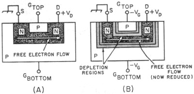
Fig. 3 - The junction field-effect transistor (JFET).
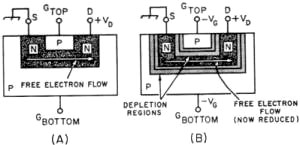
Fig. 4 - Operation of the JFET under applied bias. A depletion
region (light shading) is formed, compressing the channel and increasing its resistance
to current flow.
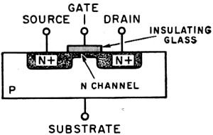
Fig. 5 - The insulated-gate field-effect transistor (IGFET).
The Junction Diode
The resulting action of a p-n junction is well known. When a forward bias is
applied as shown in Fig. 1B, a large current will flow. The total current is
made up of the electron current plus the hole current. When reverse bias (Fig. 1C)
i applied, only a small reverse current flows - the p-n junction acts as a diode.
It is important to note the reverse-bias case. We know that when a voltage is applied
to a resistive network, this voltage is dissipated by IR drops until the applied
voltage is "used up" by the sum total of all the voltage drops. The same principle
applies to the case of the reverse-biased p-n junction diode. We have applied V
volts of reverse bias and this voltage must be used up somehow in our circuit, the
p-n junction. The resulting action is shown in Fig. 2, where charges are separated
in a region close to the junction. Enough charges are moved until the electric field
across the junction produces a voltage drop which is approximately equal to our
applied voltage. The important point here is that the region around the p-n junction
is now depleted of all its holes and free electrons, thus there are no current carriers
available. This region is commonly called the "depletion region" and it sounds reasonable
that its thickness depends on the magnitude of reverse voltage which is applied.
It will be an important point in the operation of field-effect transistors that
no current can flow in the depletion region since there are no current carriers
in that region.
The Junction FET (JFET)
Field-effect transistors are divided into two main groups: junction FETs, and
insulated-gate FETs. We will discuss the Junction FET, or JFET, first. The basic
JFET device is shown in Fig. 3.
First of all, note the location of the terminals where voltages can be applied.
The reason for the terminal names will become clear later. A d.c. operating condition
is set up by starting a current flow between source and drain. This current flow
is made up of free electrons since the semiconductor is n-type in the channel, so
a positive voltage is applied at the drain. This positive voltage attracts the negatively-charged
free electrons and the current flows (Fig. 4A). The next step is to apply
a gate voltage of the polarity shown in Fig. 4B. Note that this reverse-biases
the gates with respect to the source, channel, and drain. This reverse-bias gate
voltage causes a depletion layer to be formed which takes up part of the channel,
and since the electrons now have less volume in which to move the resistance is
greater and the current between source and drain is reduced. If we apply a large
gate voltage, we cause the depletion regions to meet, and in this case the source-drain
current is reduced nearly to zero. Since we changed the large source-drain current
with a relatively small gate-voltage, we have a device which acts as an amplifier.
Further, note that in the operation of the JFET, the gate terminal is never forward
biased, because if it were the source-drain current would all be diverted through
the forward-biased gate junction diode.
The resistance between the gate terminal and the rest of the device is very high,
since the gate terminal is always reverse biased, so the JFET has a very high input
resistance. The source terminal is the source of current carriers, and they are
drained out of the circuit at the drain. The gate opens and closes the amount of
channel current which flows. It is seen how the operation of a FET closely resembles
the operation of the vacuum tube with its high grid input impedance. Comparing the
JFET to a vacuum tube, the source corresponds to the cathode, the gate to the grid,
and the drain to the plate.
Insulated-Gate FET (IGFET)
The other large family which makes up field-effect transistors is the insulated-gate
field-effect transistor, or IGFET, which is pictured schematically in Fig. 5.
In order to set up a d.c. operating condition, a positive polarity is applied to
the drain terminal. The substrate is connected to the source, and both are at ground
potential, so the channel electrons are attracted to the positive drain and we now
have a d.c. source-drain current. In order to regulate this current, we apply voltage
to the gate contact. Note that the gate is insulated from the rest of the device
by a piece of insulating glass so this is not a p-n junction between the gate and
the device - thus the name insulated gate. When a negative gate polarity is applied,
positively-charged holes from the p-type substrate are attracted towards the gate
and the conducting channel is made more narrow; thus the source-drain current is
reduced. When we connect a positive gate voltage, the holes in the substrate are
repelled away, the conducting channel is made larger, and the source-drain current
is increased. As can be seen, the IGFET is more flexible since we can apply either
a positive or negative voltage to the gate. The resistance between the gate and
the rest of the device is extremely high because they are separated by a layer of
glass - not as clear as your window glass, but it conducts just as poorly. Thus
the IGFET has an extremely high input impedance. In fact, since the leakage through
the insulating glass is generally much smaller than through the reverse-biased p-n
gate junction in the JFET, the IGFET has a much higher input impedance. Typical
values of Rin for the IGFET are over a million megohms, while Rin
for the JFET ranges from megohms to over a thousand megohms.
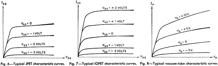
Fig. 6 - Typical JFET characteristic curves. | Fig. 7
- Typical IGFET characteristic curves. | Fig. 8 - Typical vacuum-tube characteristic
curves.
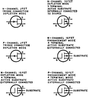
Fig. 9 - Symbols for most-commonly available field-effect
transistors.
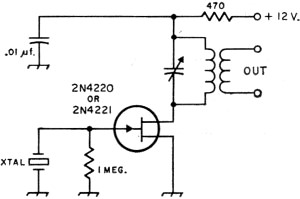
Fig. 10 - Typical JFET crystal-oscillator circuit.
Characteristic Curves
The characteristic curves for the FETs described above are shown in Figs. 6 and
7, where drain-source current is plotted against drain-source voltage for given
values of the gate voltage. Note the similarity to the family of a vacuum-tube pentode
as shown in Fig. 8, where plate current is plotted against plate voltage for
varying amounts of grid voltage.
In discussing the JFET so far we have left both gates separate so the device
can be used as a tetrode in mixer applications. However, the gates can be internally
connected for triode applications. When using the IGFET the substrate is always
a.c.-shorted to the source, and only the insulated gate is used to control the current
flow. This is done so that both positive and negative polarities can be applied
to the device, as opposed to JFET operation where only one polarity can be used,
because if the gate itself becomes forward biased the unit is no longer useful.
Classifications
Field-effect transistors are classed in to two main grouping for application
in circuits, enhancement mode and depletion mode. The enhancement-mode devices are
those specifically constructed so that they have no channel. They become useful
only when we apply a gate voltage which causes a channel to be formed. IGFETs can
be used as enhancement-mode devices since both polarities can be applied to the
gate without the gate becoming forward biased and conducting current.
A depletion-mode unit corresponds to Figs. 3 and 5 shown earlier, where a channel
exists with no gate voltage applied. For the JFET we can apply a gate voltage and
deplete the channel, causing the current to decrease. With the IGFET we can apply
a gate voltage of either polarity so the device can be depleted (current decreased)
or enhanced (current increased).
To Slim up, a depletion-mode FET is one which has a channel constructed; thus
it has a current flow for zero gate voltage. Enhancement-mode FETs are those which
have no channel, so no current flows with zero gate voltage . The latter type devices
are especially useful in logic application.
Circuit symbols approved for FETs are shown in Fig. 9. Both depletion-mode
and enhancement-mode devices are illustrated.
Applications
Some applications for FETs are shown in Figs. 10 and 11. In Fig. 10 a JFET
oscillator is pictured, and a versatile FET d.c. voltmeter (FETVM) is shown in Fig. 11.
The voltmeter features two Motorola 2N4221 JFETs and offers the high input impedance
(22 megohms on all ranges in Fig. 11) of a v.t.v.m, but with more stability.
The circuit is essentially a differential amplifier which works on the principle
that the current through a resistance is directly proportional to the difference
between the voltages at its ends. When R1 and R2 are adjusted
so that the voltage at the emitter of Q2 is equal to the voltage at the
emitter of Q3, with no input signal, the voltage difference is zero and
no current will flow through the meter.
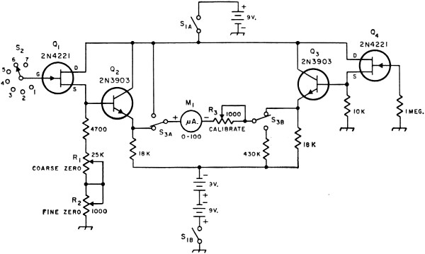
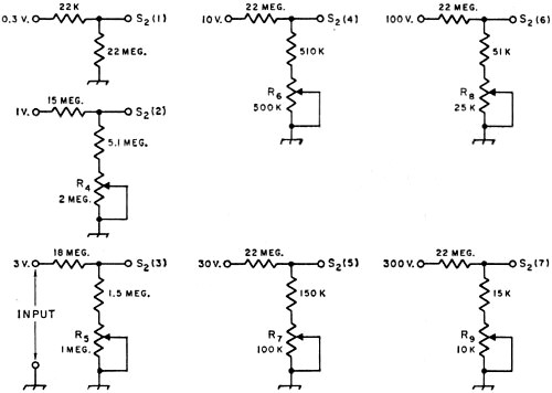
Fig. 11 - D.C. voltmeter circuit using field-effect transistor. Resistances
are in ohms (K = 1000); fixed resistors are 1/2 watt. The second position of S3
is used for checking battery voltage.
M1-0-100 microammeter. S1-D.p.s.t.
toggle. S2-D.p.d.t. toggle.
S3-Rotary, 1 section, 1 pole,7 positions. R1
R2 R3-Linear controls (R2 and R3 are
panel adjustments; R1 can be internal). R4-R9
inc.-Trimming potentiometers, for internal mounting (Mallory MTC or equivalent).
When the voltage at the gate, G, of Q1 is raised to 0.3 volt the voltage
across the meter circuit also is approximately 0.3 volt since the source followers
and emitter followers have a voltage gain of approximately one. R3 is
then adjusted to give full-scale meter deflection. The calibration resistors, R4-R9
inclusive, are individually adjusted for exactly full-scale deflection on each range
when the maximum voltage for that range is applied to the input terminals through
the range switch, S2.An accurate voltmeter should be used to check the
applied voltage when setting the calibration resistors.
These two circuits were furnished by Don Wollesen and Walter Birks of the Applications
Engineering Group at Motorola Semiconductor Products Division.
This article has provided a basic look into the FET and some of its applications.
In general, the FET offers much improved noise performance, stability, and cross-modulation
resistance over either vacuum tubes or standard transistors (p-n-p, n-p-n). Its
many features, such as high input impedance and desirable high-frequency performance,
insure its design into a vast number of electronic circuits in the near future.
It is probably the most recent radical improvement in device design, and should
prove most interesting to amateur radio operators everywhere, allowing them greatly
improved freedom in circuit design.
* c/o Motorola Semiconductor Products, Inc., 5005 East McDowell Road, Phoenix,
Ariz. 85008
Posted October 30, 2019
(updated from original post on 2/13/2013)
|