|
September 1942 Radio-Craft
 [Table
of Contents] [Table
of Contents]
Wax nostalgic about and learn from the history of early electronics.
See articles from Radio-Craft,
published 1929 - 1953. All copyrights are hereby acknowledged.
|
Television and radio facsimile
machine electronics technology was credited for aiding in the development of a new
type of scanning electron microscope (SEM)
that could image the surface of opaque object to a resolution of 100 angstroms (Å).
The television contribution part of the technology was precisely controlling a raster
path for the electron beam. The facsimile part was the knowledge of how to assemble
a printed image from streaming data. It is interesting to note that in order for
an object to be imaged via SEM, its surface must be electrically conductive. Accordingly,
non-metallic objects like bugs, plants, plastic, wood, etc., must receive a coating
of metal by a process such as sputtering. Doing so can leave a few atoms thick later
without losing too much resolution due to softening of features.
New Scanning Electron Microscope Revealed to Radio Engineers
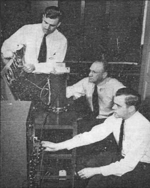
Dr. James Hillier (foreground). Dr. V. K. Zworykin (seated) and
Richard L. Snyder demonstrating the recently perfected electron microscope.
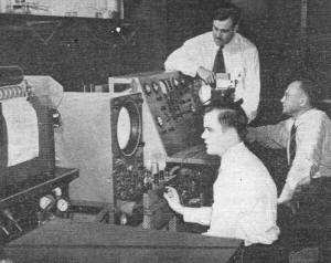
Dr. V. K. Zworykin describes perfection of new instrument at
Convention of Institute of Radio Engineers at Cleveland, Ohio.
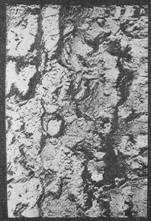
The picture from the facsimile printer of the instrument shows
etched nickel.
Perfection by a group of scientists of a scanning electron microscope which enables
the study of surfaces of opaque objects, including metal, in far greater detail
than heretofore possible, was revealed recently by Dr. V. K. Zworykin, associate
director of RCA Laboratories, in a scientific paper read at the Institute of Radio
Engineers' convention in Cleveland, Ohio. The paper was jointly prepared by Dr.
Zworykin, Dr. James Hillier and Richard L. Snyder, all of RCA Laboratories, who
contributed to development of the instrument.
While Dr. Zworykin cautioned that, as with any new instrument, it is not possible
to judge the full range of utility of the scanning electron microscope at the present
time, it was pointed out by associates that the new device has important, and possibly
far-reaching significance to the field of metallurgy. Investigation of grain structure
in metals on an order of minute detail never before realized becomes possible.
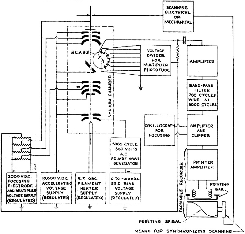
The principles of television, electron microscopy and facsimile
are joined to make this new instrument.
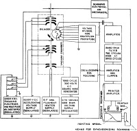
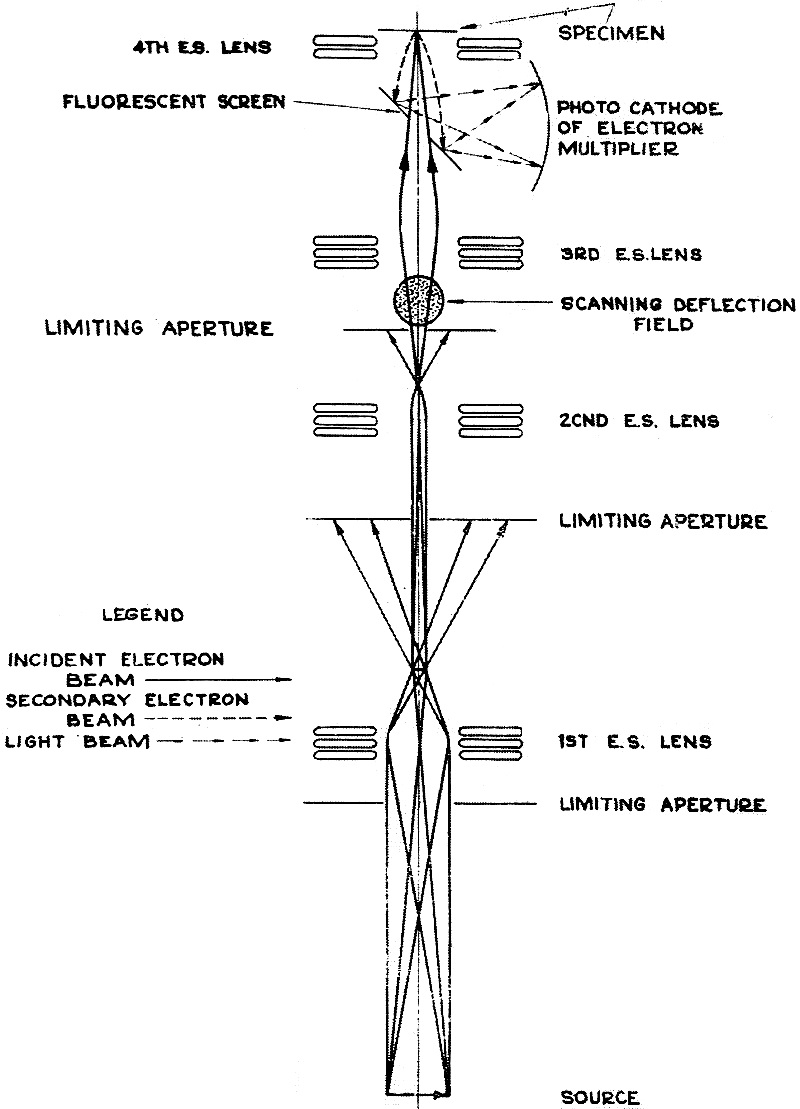
Schematic arrangement of the scanning electron microscope.

Skeleton of the new electron microscope, showing the placement
of lenses in relation to the electron beams.
The scanning electron microscope, Dr. Zworykin said, is the result of utilizing
principles and devices taken from three outstanding developments in radio and electronics
- television, the electron microscope and radio facsimile.
"Think how stupendous the undertaking would be," said Dr. Zworykin, "if someone
were to conceive an electron scanning microscope and then set out to research for
it without having the knowledge at his fingertips which we have of television and
electron microscopes, as well as the art of radiophoto or facsimile. It would be
an endless task.
"But, as often happens in science, the discovery of one good thing leads to another.
In addition to the developments mentioned, the electron multiplier tube is another
vital factor in this latest scanning achievement. After passing through an intricate
process of magnetic scanning, the electron beam containing the picture information
is converted to light at a fluorescent screen. The light is concentrated by a wide-aperture
lens on the photo-cathode of the multiplier, which in turn operates a printing device."
Explaining how the new instrument works, Dr. Zworykin said that the formation
of an image may result from one of two methods. One is the simultaneous imaging
of all the elements, as in the projection by optical lenses of a picture on a screen,
on a photographic plate, or on the retina of the human eye. The second method is
by the successive recording of individual image elements, the process used in television.
"Modern high-power electron microscopes may utilize either of these procedures,"
Dr. Zworykin said. "The conventional electron microscope - also perfected by RCA
Laboratories - like any ordinary optical instrument, records the entire array of
elements simultaneously in the form of an electron-optical image. The scanning microscope,
however, adopts the methods of television, that is, records one picture element
at a time..."
Each type of electron microscope has its own particular sphere of usefulness,
Dr. Zworykin pointed out. The conventional electron microscope, he said, is primarily
suited for the study of "transparent" objects, specimens less than a micron in thickness;
while the scanning microscope has as its special province the investigation of the
surface of objects, which are opaque to electrons. Roughly, the two types of electron
microscopes correspond in application to the light microscopes used in biological
and metallurgical work, but the electron instruments "see" much greater detail.
"As simple as the basic principle of the scanning electron microscope may appear,"
continued Dr. Zworykin, "the realization of an instrument with a resolving power
comparable with that of the electron microscope was confronted with very great difficulties.
These obstacles arose from the necessity of making the scanning spot no larger than
the least separation which is to be resolved, that is, no larger than one two-millionth
of an inch (100 Angstrom Units) in diameter. It was no easy job to form a spot of
this size, but we have succeeded."
In fact, so accurate and delicate is the control of the electrons in passing
through the instrument to help "see" the surface of the metal, or object being observed
and photographed, that the tiny electrons pass through the scanning tube about one
yard apart. The mastery achieved is indicated further by the fact that, theoretically,
it would require 30 billion, billion, billion of electrons to weigh an ounce.
The scanning electron microscope was brought to perfection by research and development
work which extended over a period of years, and was participated in by a large number
of scientists in RCA Laboratories. The authors of the paper, Zworykin, Hillier and
Snyder, called particular attention to the early work of Arthur W. Vance and L.
E. Flory, and to the mathematical contributions of Dr. E. G. Ramberg, all of RCA
Laboratories.
A summary of the technical paper prepared by the authors follows:
In order to examine the surface of bulk material with the high resolving power
afforded by the use of an electron beam a new electron microscope of the scanning
type has been developed in which an extremely fine and stationary electron probe
is produced by a two-stage reducing electrostatic-lens system. The specimen is moved
mechanically in such a way that each point of its surface is scanned in a systematic
fashion by the electron probe. The secondary electrons which are emitted from the
point of the specimen bombarded by the electrons of the probe are accelerated and
projected on a fluorescent screen. The intensity of the light emitted by the fluorescent
screen varies in accordance with the secondary-emission properties of successive
points of the specimen. This modulated light signal is converted into an electrical
signal by means of a multiplier phototube and then synthesized in a printed picture
by an amplifier and facsimile printer system. The use of the electronic-light-electronic
transformation of the image signal improves the signal-to-noise ratio by at least
an order of magnitude over that found in conventional methods of collection and
voltage amplification. An experimental model has been constructed and has been successful
in producing images of etched metal surfaces at magnifications as high as 10,000
diameters and with a resolving power considerably better than 50 millimicrons. The
blackening of the image points has been found to be a function of the three-dimensional
contour of the specimen as well as of its secondary-emission properties.
Posted September 14, 2021
(updated from original post on 10/19/2014
|