|
May 1969 Radio-Electronics
 [Table of Contents] [Table of Contents]
Wax nostalgic about and learn from the history of early electronics.
See articles from Radio-Electronics,
published 1930-1988. All copyrights hereby acknowledged.
|
A nice article by Donald Lancaster
appeared in an issue of Radio-Electronics magazine that introduces and
puts into layman's terms the relatively new (at the time) world of digital logic
circuits. Rapidly falling prices and equally rapidly rising performance fuelled
the craze. By 1969, most of the barriers preventing former never-tubers from adopting
the fledgling semiconductor paradigm and there was by then a new generation of electronics
hobbyists, technicians, and engineers who had "grown up" on transistors and integrated
circuits. I like the author's analogies for AND gates and OR gates that involve
the familiar objects that include a garden hose with the house tap and nozzle, and
the kitchen sink faucet with the hot and cold handles. It's interesting how often
water, a substance generally to be avoided around electricity, is used in analogies
about voltage and current flow. Yes, I realize that pure water is an excellent insulator,
but most coexistences of water and lethal electricity levels involve impure water.
Low-cost computer logic gates make 'everyday' circuits easy to build
By Donald Lancaster
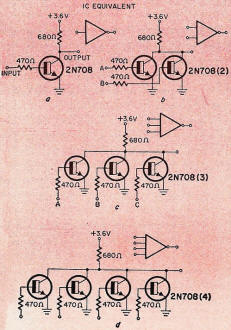
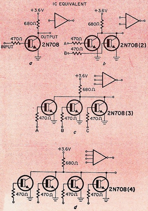
Fig. 1-a - This is a one-input RTL logic gate and its IC equivalent
symbol. Parts b, c and d are two- three- and four-input gates respectively with
their IC symbols. All circuits run as saturated-logic switches. When any base receives
current, the output of that gate goes near ground. If all bases do not receive current,
the output goes positive to 3.6 volts.
Price reductions on many digital integrated circuits have made the logic gate
practical for many "everyday" circuits. Besides their obvious use as computer logic
elements, these gates readily form the active elements needed for conventional pulse
and digital circuits, multivibrators, triggers and a host of other circuits.
By adding a biasing resistor, logic gates may be made into class-A linear amplifiers,
useful in many low-level applications. Let's look at some of the more popular gates.
What's Available
There are many advantages in using IC logic gates to replace conventional transistors,
resistors and diodes. Foremost is cost. One $1.08 package, for example, contains
six complete integrated gates - only 18¢ per gate. This is far less than the price
of a single transistor or diode.
As logic gates may be directly connected together and require no biasing or coupling
circuitry, the need for external resistors and capacitors is greatly reduced. Logic
gates are very compact, with two to six in a single plastic package. Circuit design
is greatly simplified, since you know operating temperature range, speed, drive
capability and power requirements ahead of time. For many applications, one or two
penlight cells operate the circuit.
A logic gate obeys certain rules to turn an output off or on upon some coincidence
of signals at its input. A kitchen sink faucet is a logic gate - it gives you an
output if either the hot or cold input is provided with an on signal. This is an
example of an OR circuit. A garden hose is an example of an AND logic gate, since
both the outdoor faucet and the nozzle valve must be on to get an output.
There are many forms of logic gates: mechanical, hydraulic, chemical, pneumatic,
optic, electric and electronic. The electronic logic is far and away the most prevalent;
millions upon millions of gates are used in the computer industry. Integrated circuits
were called upon a decade ago to reduce the size, cost and power consumption of
computers.
As a result, many forms of IC logic gates are available today. Those we'll talk
about are called RTL gates, because they are the integrated equivalent of Resistor
Transistor Logic. Fig. 1 shows the discrete equivalent circuits for the one-, two-,
three- and four-input RTL gates and their integrated equivalents.
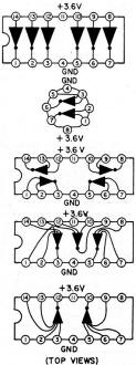
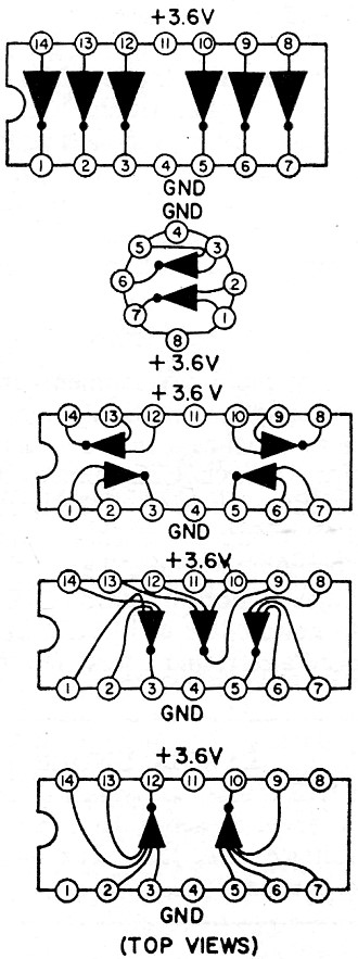
Table I - A few of the gate combinations available in 14-lead
"caterpillar" and 8-lead TO-5 cases. Top to bottom: Hex inverter, dual two-input,
quad two-input, triple three-input, dual four-point. In each case, gates are independent.
The two-input gate consists of two npn transistors sharing a common-collector
resistor. Each base has a current-limiting resistor attached to an input. If either
input receives base current, the output goes to ground. If neither input receives
base current, the output goes positive to the supply voltage.
Using this basic configuration and choosing our definitions carefully, we can
interconnect logic gates to perform all computer functions, and any set of logic
rules we wish.
A few of the more popular gates available are IC's that come in an eight-pin
TO-5-size epoxy package or a 14-lead in-line "caterpillar" package. Both types are
interchangeable and operate from a single +3.6-volt supply. For many applications
1.5 -4.5-volt battery supplies will work as well. The gates have a transition time
around 15 nanoseconds. This is very slow as computer circuits go, but for everyday
applications the gates are useful from DC to beyond 10 MHz.
Note that all the packages contain more than one gate. All the gates are independent,
and the only common connections are supply voltage and ground. For instance, a quad
two-input gate contains four independent gates, each gate being the two-input variety.
A dual four-input gate has two separate gates, each of which has four separate inputs.
Pin conventions are shown in Table I. The eight-pin version has a flat or color
dot adjacent to pin 8, while the in-line package has an identifying notch and top-view
pin connections as shown. IC's are good over a +15°-55°C temperature range.
Each gate consumes about 12 mW of supply power. Each gate's output can drive five
similar gate inputs; where more output power, or fanout, is required, a different
IC, called a buffer, is needed.
Logic Circuits
What integrated logic gates will do in computer applications depends, not only
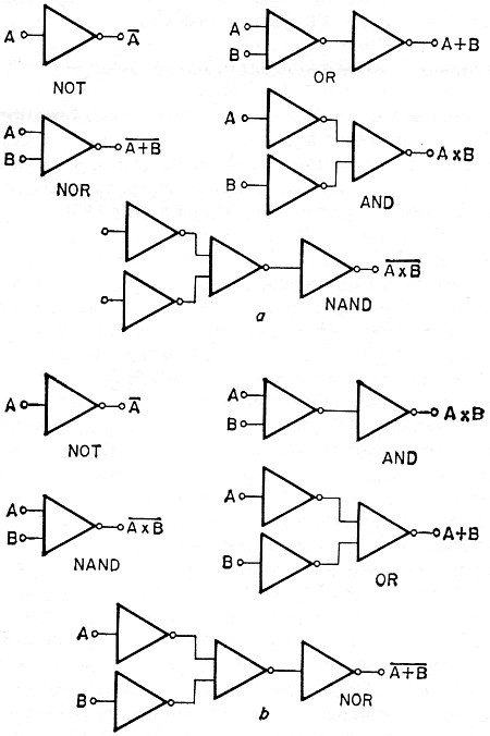
on the circuit connection, but also on definitions. For example, if we define" +"
as "1" and ground as "0," we are using a positive logic gate, and the NOT, NOR,
NAND, OR, AND logic gates are built up with circuits of Fig. 2 - a. If, on the other
hand, we define ground as "1" and "+" as "0," we are using negative logic, and the
NOT, NAND, AND, OR and NOR functions are generated with the different gate connections
shown in Fig. 2-b.
To analyze any logic function, consider what the actual gate does. The NAND coincidence
is based upon neither transistor receiving base current, thus allowing the output
junction to swing positive. The NOR coincidence is based upon any gate transistor
receiving base current and thus forcing the output junction to ground.
As an example of a more complicated computer logic circuit, the EXCLUSIVE OR
circuit, also known as a half-adder, is shown in Fig. 3. This circuit directly performs
binary addition. Usually two half-adders are used together, one to add two binary
numbers and a second to handle a possible carry from the previous addition. Note
that a considerable number of inverting gates may be eliminated, if the complements
of the input and output are available or useful elsewhere in the circuit.
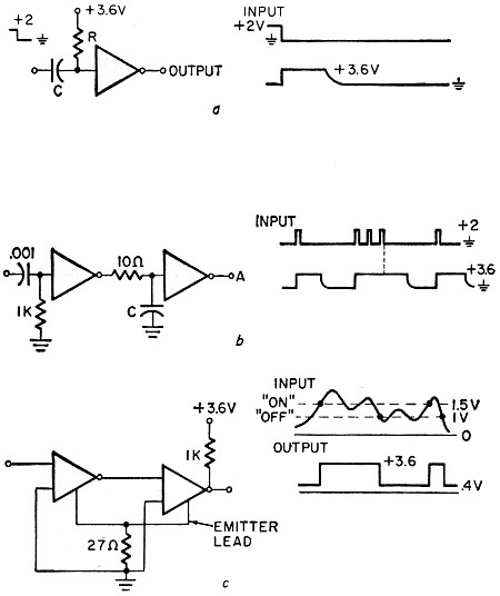
Suppose we connect two one-input gates back to back as in Fig. 4-a. If the left
gate's output happened to be grounded, it would allow the right gate's output to
be positive, which in turn would provide the base current to keep the left gate's
output grounded. The circuit is stable and, if undisturbed will stay in either of
the two possible states. This is called a bistable multivibrator.

Fig. 2 - Computer logic functions depend on definitions. Top
(a) drawings show positive logic: "1" is positive and "0" is ground. In negative
logic (b), "1" is ground and "0" is positive.
The circuit is more useful if we force the bistable to go into either of the
two states upon command. This is done by adding two push buttons as in Fig. 4-b.
Push the SET pushbutton, and point A goes to ground and stays there after the button
is released. Push the RESET button and point A goes" +" and point B goes to ground,
and stays there after the button is released. We can use this circuit as a memory
or latch; it is somewhat similar to a relay latching itself on its own make contact.
It is often desirable to change states upon electrical command. For this, we
go to the two-input gate configuration of Fig. 4-c. Here one gate input on each
side is used for feedback; the other for an input. A short positive pulse at either
input then sets or resets the latch, depending upon the input selected.
For the circuit to operate properly, the inputs must "see" a DC return path and
the input pulses must be brief. To ac-couple signals, or to trigger on the leading
edge of a long input pulse, requires the pulse coupling circuit of Fig. 4-d. The
1000-ohm resistors are essential; if they are omitted, the gate's base-emitter pn
junction will act as a DC restorer and charge up the input capacitor after one or
two operating cycles.
If input signals appear simultaneously, both outputs wilt go to ground and the
last input to disappear determines the state the bistable will go into.
The circuits shown will not count and will not automatically steer input pulses
from one side to the other if the inputs are connected together. To do this, an
integrated circuit called a JK flip-flop is needed.
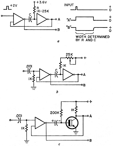
Monostable Circuits
Suppose we break one of the feedback connections of the latch and insert a capacitor
and recharging resistor (Fig. 5-a). If we let the circuit sit long enough, it will
go into the state in which the left gate's output is positive and the right output
is grounded. Capacitor C will charge to roughly the supply voltage.
Now, if an input trigger pulse is delivered, the left gate's output will immediately
go to ground. Since the charge on a capacitor cannot immediately change, the right
end of C abruptly drops negative, removing base current from the right gate. The
right gate's output swings positive, and thus provides base current for the left
gate, holding the circuit in the new state.
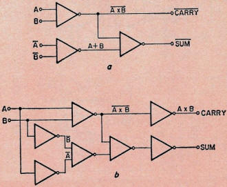
Fig. 3 - The Exclusive OR circuit (half adder) is one of the
more complex computer functions. Part a shows arrangement with usable complements
available; b has self-generated complements.
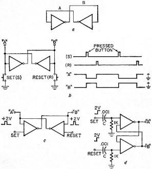
Fig. 4 - Various configurations of bistable multivibrators. In
a, two one-input gates are back to back. Part b shows same circuit wired for pushbutton
operation. Circuit in c uses two-input gate for a pulse set-reset latch. The pulse-coupling,
set-reset flip-flop in d triggers with long input pulse.

Fig. 5 - These are monostable multivibrator and delay circuits.
Basic circuit in a requires a brief, de-coupled input. With circuit in b, the output
is variable over a 10:1 range. High-gain transistor in c permits long time delays
of output.
So far things have gone just as they did in the bistable circuit. But resistor
R now starts charging the right end of C positively, until the voltage on the right
end of C is positive enough to provide base current for the right gate. The right
gate's output starts to ground, and the circuit snaps back to the original state.
This is another form of multi vibrator. It has one stable state and one unstable
one. Called a monostable multivibrator, it is used to generate a time delay or a
rectangular pulse of controlled width upon command. To vary the output width or
delay, R or C is varied. A 10:1 range is obtained by the circuit of Fig. 5-b. Here
we have also added input capacitors for AC coupling or for triggering an input that
is long compared to the delay time.
There are several important design considerations. The input signal (either directly
or through the capacitor differentiation network) must be brief compared to the
delay time, or the circuit will not operate properly. As with the bistable circuit,
the 100-ohm resistor on the input is essential if capacitor coupling is used. The
timing resistor may vary from 1000 to 25,000 ohms, while C may range from 200 pF
up to several hundred microfarads. The time constant of RC roughly equals the delay
time, with intervals from 200 nsecs to several seconds possible.
The monostable has a recovery time. It cannot be immediately retriggered, since
C must recharge completely to the supply voltage. Constant-width operation may be
obtained with a duty cycle less than 30%, while a duty cycle as great as 75% may
be used if considerable change in timing is permissible. The generated pulse width
does not vary greatly with small changes in temperature or supply voltage.
Time intervals longer than a fraction of a second require unreasonably large
values of C as resistor R cannot be made larger than 25,000 ohms without running
out of gain in the second gate. For long time intervals, a gate may be combined
with a very-high-gain transistor to allow a much larger value of R, and a resultant
reduction in capacitor size. (Fig. 5-c).
Other Trigger Circuits
Figure 6-a shows a nonregenerative pulse stretcher that provides a monostable
output with a single, one-input gate. It produces a rectangular output pulse upon
command, and is used only when the input is decoupled and goes to ground and stays
there for a time longer than the pulse period. Since there is no feedback, the fall
time is not nearly as good as can be obtained with a true monostable.
To trigger the circuit, the input is made positive long enough to charge C. The
input is then abruptly brought to ground and held there. Since the charge on C cannot
change instantaneously, the right end of C swings negative, turns off the gate and
produces a positive output. Resistor R then charges C just as in the conventional
monostable.
A monostable circuit with "negative" recovery time is shown in Fig. 6-b. Here
the output goes positive immediately upon an input command and stays positive for
a time delay determined after the last pulse or input command chain is received.
An input pulse discharges C, which then recharges through the internal collector
resistor of the right gate until it is positive enough to allow the right gate to
turn on. As C is "emptied" each time an input pulse arrives, the time delay begins
anew with each input pulse.
The output fall time is not very good, and very large C values are required for
millisecond pulse intervals. The circuit is also rather dependent on supply and
temperature and requires input pulses long enough to discharge C completely. One
interesting application for this circuit is with voice-operated relays. Another
is for missing-pulse detection or producing an output only after an entire string
of input pulses has passed.
A Schmitt trigger is shown in Fig. 6-c. This is an emitter-coupled multi vibrator
that is sensitive to input voltage. As the voltage exceeds a given level, the Schmitt
circuit snaps into one state. As the voltage drops below a second level, the circuit
snaps back into the original state.
The two levels are made different, producing hysteresis and eliminating chatter
or noise sensitivity. The circuit shown snaps on with an input exceeding 1.5 volts,
and off with the input voltage dropping below 1.1 volts.
Since the ground lead must be broken and a 27-ohm resistor inserted in series
with the negative return on the IC, the circuit will work only with a dual two-input
gate. The 27-ohm resistor determines the trip points, while the output resistor
determines the amount of hysteresis obtained. The circuit is used as an alarm or
a voltage-level detector. Signal conditioning of the output may be required before
driving additional logic gates.

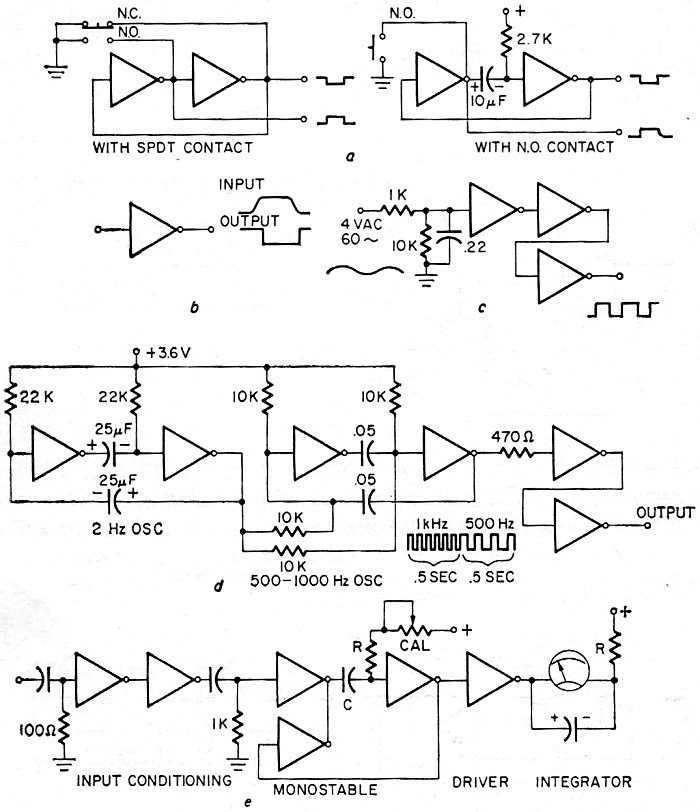
Fig. 6-a - Nonregenerative pulse stretcher in this circuit requires
an input staying at ground for duration of the output. The nonregenerative monostable
in b is controlled by last pulse in input chain. A Schmitt trigger is shown in d.

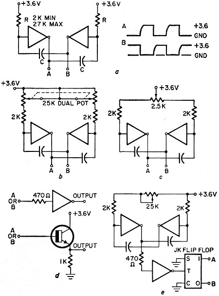
Fig. 7 - Various free-running multivibrators: Circuit a is a
basic astable, b is astable with dual-pot frequency control, c has variable symmetry
output. Part d shows resistor and transistor load isolation; e shows JK flip-flop
division by 2.
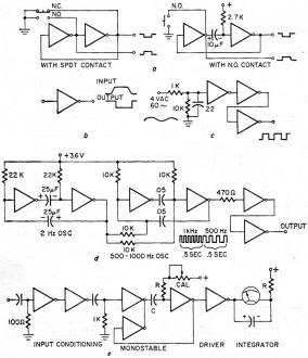
Fig. 8 - Here are a few practical applications. Part a shows
bounceless pushbuttons (spdt on left, and n.o. on right). A squaring circuit is
in b, and a 60-Hz driver for high-speed JK's is in c. Single IC in d can be two-tone
oscillator or alarm. A hex-inverter tachometer is shown in circuit e.
An astable multi vibrator has no stable state and is thus free-running, forming
a square-wave oscillator circuit (Fig. 7-a). Once again, timing is determined by
the RC products. The waveform will be asymmetrical unless the RC products are equal.
Fig. 7-b adds a dual 25,000-ohm potentiometer to obtain a 10:1 control range. For
wider ranges, various values of C are switched in. There does not seem to be any
starting problem with an IC astable of this type.
The circuit of Fig. 7-c provides a fixed output with variable symmetry. The minimum
recommended value of R is 2000 ohms; the maximum, 25,000 ohms. Capacitor C may vary
from 200 pF up to several tens of microfarads.
The circuit operates properly only if lightly loaded. Two load-isolating techniques
are shown in Fig. 7-d, one of which requires a resistor and a gate, the other a
transistor emitter follower and a resistor.
Single-potentiometer operation will result in a highly asymmetrical waveform.
A very nearly square wave with excellent symmetry may be obtained by dividing the
astable multivibrator's output by 2 with a JK flip-flop; the flip-flop's output
is perfectly symmetrical, except for a possible small transition time (Fig. 7-e).
Some Applications
Let's look at how we can use these logic gates in other useful circuits. Fig.
8-a shows two bounceless push-button circuits, essential whenever mechanical contacts
are used with high-speed integrated counter circuits. A dual circuit or an spdt
pushbutton may be used to drive a set-reset bistable multivibrator directly. This
circuit requires two one-input gates. If an spst or make contact is the only one
available, the 15-msec multivibrator circuit may be used. This requires an additional
resistor and capacitor.
A single one-input gate is used as a squaring circuit to sharpen rise and fall
times of an input signal (Fig. 8-b). Around 20 nsecs of delay will also be picked
up, and a single gate can be used as an ultra-short delay line. Fig. 8-c shows a
filter and three cascaded one-input gates. This circuit is used to square 60-Hz
power-line or other low-frequency audio sine waves. The output is a square wave
with a very fast fall time, a feature essential when integrated JK flip-flops are
to be used in low-frequency circuit applications.
The dual-tone oscillator of Fig. 8-d produces a commanding alarm that switches
between 500 and 100 Hz twice each second. In operation, the left two gates operate
as a 2-Hz oscillator that alters the charging current and hence the frequency of
the high-frequency astable formed by the middle two gates. The remaining gates serve
as load isolation. The circuit drives any amplifier; with a companion driver transistor,
it will directly drive a speaker to ear-splitting volume. Note the extreme simplicity
possible by using a hex inverter - only one active component is needed for the circuit.
The same hex inverter is useful in tachometer circuits, again with a significant
parts reduction. Fig. 8-e shows the technique. By keeping the monostable duty cycle
well under 30% and isolating the indicating meter from the monostable, a considerable
improvement in stability over simpler circuits is obtained. As with any pulse duty-cycle-type
tachometer, the supply must be regulated and a suitable input network must be chosen
to isolate ignition spikes and noise.
Linear Operation
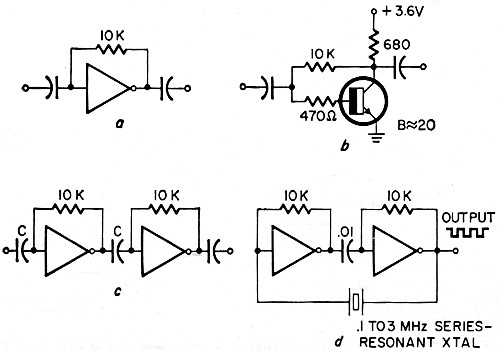
Gates may be biased up into the class-A region to produce a very-low-cost linear
amplifier. Fig. 9-a shows the biasing scheme, while Fig. 9-b shows the approximate
equivalent circuit. Discrete versions of this circuit are not often seen as the
input impedance is rather low - even though the configuration has good gain and
bias stability. The stages may be cascaded.
AA gain-of-400 amplifier is shown in Fig. 9-c. Note that coupling capacitors
are essential to keep the proper bias levels on each stage. Up to three stages may
be cascaded, producing gains above 60 dB. Maximum linear peak-to-peak output is
around 1 volt. A practical application of the class-A technique is the crystal oscillator
of Fig. 9-d, which produces square waves at the fundamental resonant frequency of
a series-resonant crystal.
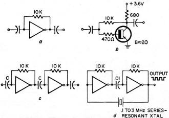
Fig. 9 - Biasing scheme for class-A amplifier operation of gates
is shown in a and the equivalent circuit in b. Circuit in c is gain-of-400 amplifier,
and d is a crystal oscillator.
Posted May 7, 2019
|