|
May 1969 Radio-Electronics
 [Table of Contents] [Table of Contents]
Wax nostalgic about and learn from the history of early electronics.
See articles from Radio-Electronics,
published 1930-1988. All copyrights hereby acknowledged.
|
Stanford R. Ovshinsky is a name with which most people are probably not
familiar, even though some of his 400+ patented inventions can be found in many
products. The most notable is the nickel-metal hydride (NiMH) battery. He also
delved deep into phase change memory and amorphous semiconductors. What caught
my attention in this 1969 Radio-Electronics magazine article was the
claim that use of an ovonic switch matrix in conjunction with red, green and
blue (RGB) phosphor light sources could produce the world's first large screen,
flat panel video display that would not require scanning electron beams or rear
projection. History shows that the idea never came to market, probably due to a
combination of technical, financial, and manufacturability issues. Ovonics (a
portmanteau
of "Ovshinsky" and "electronics") is still used in aspects of the alternative
energy industry.
Here is a news item about
Ovshinsky
in the January 1969 issue of Radio-Electronics
All About Ovonics & How to Use Them
Glassy semiconductor switch! Is it new? Is it a breakthrough? Or is it nonsense?
by Fred Shunaman
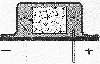
Fig. 1 - If ovonic material is placed between two electrodes
and a voltage is applied, the voltage exerts a pull on the trapped carriers, marked
e in figure.
"The newest, the biggest, the most exciting discovery in solid-state physics
at the moment" was heralded in front-page articles in the daily press a few months
ago. The transistor, the articles screamed, was about to be superseded by a new,
smaller, lower-cost, and more reliable device; a device that would make it possible
to have computers so small and so inexpensive that every two-car family could have
one; a device that would finally make the picture-on-the-wall TV set a reality.
A self-educated inventor, Stanford R. Ovshinsky of Troy, Michigan, had announced
that he had obtained patents on a new type of semiconductor switch, one that did
not have to use crystalline semiconductors, but was made of disordered (amorphous
or formless) materials or glasses. These switches could be operated by any voltage
from about 2.5 to 300 or more, would switch in picoseconds, and - unlike transistors
- were bilateral (would work both ways).
Even more important, the new devices were insensitive to radiation and could
be used in space equipment. Another possible use was on nuclear warheads. Most antimissile
weapons depend on paralyzing the electronics of a warhead with radiation. War-heads
equipped with Ovshinsky's devices would ride right through a strong radiation field
without noticing it.
A few days later, the same papers came out with more subdued stories. Reporters
sent out to interview large electronics companies found little enthusiasm. "Yeah,"
the manufacturers said in effect, "we know about them. They work - after a fashion."
One large company reported using the devices experimentally; another had been a
licensee of Ovshinsky's firm for a few years. One outfit even claimed to have invented
the device - years ago!
So, what is the truth? What is this Ovshinsky device? Will it work? How? What
can we expect from it? Is it new? Is it revolutionary? Is it even Ovshinsky's?
A True Semiconductor Device
First of all, it is a semiconductor. It is a two-terminal device, so it might
be called a diode - except it is a two-way device, conducting equally well both
ways. Physically, it has a very thin "glass" film. (One formula is 48% tellurium,
30% arsenic, 12% silicon and 10% germanium.) If a voltage is connected across this
semiconductor, it acts like a high resistance (hundreds of megohms) until the voltage
reaches a certain point. Then the resistance drops suddenly to as little as 6 ohms
or less.
Depending on the thickness of the layer and its composition, the trigger or threshold
voltage varies from about 2.5 to over 300 volts. Since the semiconductor is practically
an open circuit until it is triggered, almost no power is needed to turn it on,
even at the 300-volt threshold. And since the resistance can drop to a few ohms
once triggered, it can handle large amounts of current - in the order of amperes.
Fig. 2 - Two wires coated with thin film of ovonic semiconducting
material may indicate the ultimate in solid-state switching. Cost reflects simplicity.
Why Does It Work That Way?
This is one of those "good" questions. Strangely enough, less is known about
noncrystalline (amorphous) solids than crystals. This is largely because the orderly
and symmetrical arrangement of the crystal structure lends itself to mathematical
treatment. A few theoretical physicists have devoted themselves to the more rugged
and less popular task of studying amorphous solids. The ovonic device is one of
the first fruits of their efforts.
One of the things researchers of "disordered structures" found out is that (in
the words of Jan Tauc of the Czechoslovak Academy of Sciences): "In an amorphous
body or in a liquid the atomic arrangement is not totally chaotic. The chemical
forces between the atoms tend to bind the atoms in the same way they are bound in
a crystal. The consequence of these forces is that the arrangement of the nearest
and next-nearest neighbors of a given atom is not very different from that in a
crystal." This finding has added some order to an otherwise disordered subject.
Mr. Ovshinsky looked for materials that would trap many carriers of electric
charge and yet, upon application of an electric field, release the carriers so that
the material can be reversibly and selectively transformed from a nonconductor to
a conductor.
In other words, if ovonic material is placed between two electrodes and a voltage
is applied, as in Fig. 1, the voltage exerts a "pull" on the trapped carriers (shown
as electrons, marked "e" in the figure). At a certain (threshold voltage) many carriers
are pulled out of the traps and give the previously insulating material a metal-like
quality, - it has many free carriers. This permits easy movement of carriers from
one electrode, into the semiconductor material and out into the other electrode.
Once a path is established, an avalanche of carriers starts, and the resistance
of the semiconductor drops to a few ohms. The whole process may take only about
150 picoseconds (0.000000000150 second). The conducting state is maintained until
the current drops below a given level (0.5 mA), then the material switches back
to the high-resistance condition. If the voltage is alternating, current starts
in the opposite direction as soon as threshold voltage has been reached on the opposite
alternation.
Note that when the switch goes "on" it immediately passes full current. Thus
a scope photo of the action looks like Fig. 2. (This pattern, by the way, is used
as the graphical symbol for the device, which no one so far has dared to call an
"ovistor.")
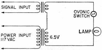
Fig. 3 - Typical application uses ovonic switch to control basic
lamp circuit.
A Memory Cell
Ovonic devices may be made in two main types. Besides the off-on switch, a unit
can be made that, once it is conductive, remains conductive even after the voltage
is removed. This effect is achieved by reducing the amount of arsenic in the material
to about 5%.
Since such a unit can remain in either one of two stages-conducting or nonconducting
- it can be used to store binary numbers. It is, in fact, a near-perfect memory
cell for computers. It can be "read out" by sending through it a current just strong
enough to determine whether it is conductive or not. This can be done without destroying
the information it carries (changing its state). The device will remain indefinitely
in its conductive or nonconductive state without any power; it can be reached immediately
to retrieve information, and can be erased by another pulse.
Indeed, a complete digital computer could be built with just these two elements
(the off-on switch and the memory device, replacing all the transistors and diodes
of a present-generation computer. This was the basis for newspaper reports of "desktop
computers for use in homes."
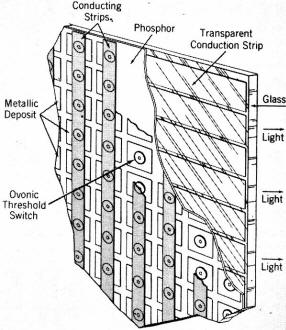
Fig. 4 - Flat TV display using ovonics might take the form shown
here. Laminated sandwich structure (closely packed transparent vertical conductors
on one side, ovonic material and phosphors in the middle, and horizontal conductors
on other side) is secret.
What Can We Do with It?
What can we do with a unit that has two terminals, will turn on when voltage
reaches a certain point and then conducts almost like a piece of wire? A mere voltage-operated
switch?
Not quite. Even if it were simply a voltage-operated switch, it would have (and
does have) an important application in computers. And this switch can be smaller
than the diodes now used, and is bilateral.
But it can control far more than the amount of power that switches it on. Suppose,
for example, we want to light a 6.3-volt lamp using about 2 watts of power, and
have a 1-volt signal (say an audio tone or the amplified signal from a vibration
transducer) with current in the milliamperes to turn it on with. We could supply
a steady 6.5 volts (ac or dc) and put our trigger signal in series with it, as in
Fig. 3. Now, when the signal voltage is added to the regular "bias" we have more
than 7 volts. An ovonic device with a 7-volt threshold will turn and supply the
full 6.5 volts (minus circuit drops) to the lamp.
The device can be made to have almost any desired threshold between 3 and 300
volts. Therefore, it can be used to release very large amounts of power with a triggering
impulse in the milliwatt range. It can also be used as a phase control to cut the
power to a circuit or appliance. If a device with a threshold of 70 volts were used
in a 120-volt line, it would work exactly like a silicon controlled rectifier (SCR)
set to turn on at 70 volts (except that it would work on both halves of the cycle).
Or a phase control somewhat similar to those used with thyratrons or SCR's could
be used to supply the turn-on pulse at a desired point in the cycle.
And that TV on the wall? (Some work along this line has already been done for
the Air Force.) By building up a laminated "sandwich" structure (closely packed
transparent vertical conductors on one side, a thin film of ovonic threshold switching
material and electroluminescent phosphors in the middle, and closely packed horizontal
conductors on the other side-see Fig. 4) it would be possible to build a flat TV
display.
Correct negative voltage applied to a horizontal conductor and positive voltage
to a vertical conductor would cause the ovonic material to "fire" at the crossover
point, creating a dot of light. By scanning, a complete picture could be built up.
Simple, but not too easy to work out for entertainment-type picture quality, though
it might do very well for a low-resolution display.
Linear Amplification
At first glance, it would seem that an all-or-nothing device like this would
be useless in any application - an audio amplifier, for example - where the amplified
signal must be varied continuously in strength. There are, however, ways to amplify
variable-amplitude signals with fixed-output devices. Pulse-code modulation is one
method; another is pulse-width modulation. The class-D or two-state audio amplifier
(Radio-Electronics July 1965, page 54) switches transistors from cutoff to full
power, varying the width of pulses presented to the final or switching amplifier
to obtain the variable audio output.

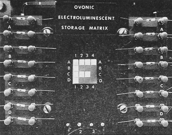
Demonstration model of ovonic electroluminescent display. In
later models, switches will be integrated with the lamps to form a fully integrated
flat panel visual display. Perhaps this will be a route to thin-screen hang-on-wall
color TV.
An Oscillator?
Ovshinsky says: "Even in a circuit stabilized with a 100-megohm load resistor,
the unit cannot be held at an operating point between the highly resistive and the
conducting state. In some cases relaxation oscillations governed by the load resistor
and the unit's capacitance have been observed."
Anyone who has ever worked with a neon-bulb stabilized power supply of the type
popular in amateur circles some years ago will understand the above perfectly. The
voltage rises till the unit just becomes conductive. Then (unless you have a perfect
zero-impedance power supply) the sudden rush of current drops the voltage slightly,
and the unit goes into the nonconductive state. This causes the voltage to rise
again, the unit becomes conductive ... and so on.
It might be interesting to see what could happen with an inductor substituted
for the load resistor. With a switching time in the picosecond range and an internal
capacitance of only 3 pF, some pretty high frequencies should be attainable.
An important feature of the ovonic unit is that-unlike other solid-state devices
- it is uniquely adapted to thin-film circuitry. There is no problem in integrating
it onto a thin-film substrate - it is thin-film itself! This is very important,
and may be a decisive factor in large-scale integration.
Another feature is its invulnerability to X-rays or other radiation from antimissile
missiles. In a crystal structure, such as a transistor, radiation may knock the
arrangement out. But since the atomic arrangement inside the ovonic device is already
that of a "perturbed crystal" radiation doesn't bother it. The radiation merely
rearranges the atoms without making it any harder (or easier) for charge carriers
to get through the structure.
This disordered arrangement is also a key to the low cost of producing the device.
No careful crystal growing, purifying or doping is needed. And not being harmed
by factors that might break down the structure of a crystal and disable it, the
ovonic device can be more reliable.
Is It Really New?
It is new to the general public. If it is new to the engineer or technician,
it is partly his own fault. Mr. Ovshinsky has been talking about it since the early
'60's without attracting too much attention. He had two handicaps: First, to avoid
patent interferences, he avoided giving details until his patents were issued recently.
(A person who says, "I have a great discovery," then fails to tell how it works
is usually suspect.) Second, although Mr. Ovshinsky has gone far in the fields of
mechanical engineering, neurophysiology and electronics, he is self-educated - has
no Ph.D. And unfortunately too many scientists are inclined to pay little attention
to a paper not authored by a Dr.
Mr. Ovshinsky's first patent on an amorphous semiconductor was granted in 1961.
However, he gives credit for the discovery of the intrinsic behavior of amorphous
semiconductors to the physicists A. F. Ioffe and B. T. Kolomiets, and much work
in the field has been done by Russian physicists. On the other hand, all his colleagues
appear to give him full credit for the voltage-switching, or Ovshinsky effect in
disordered materials.
The magazine Electronics printed an article describing the experimental use of
ovonic devices in computer circuitry in July, 1967. The story contained four pages
of color pictures of Ovshinsky's Energy Conversion Devices factory at Troy, Mich.
Will It Work?
It is already working, and in certain specialized uses, such as radiation-resistant
applications, probably better than other available devices. How far it will go in
other fields in which present-day transistors and diodes are firmly established
(or in areas totally unforeseen today) is a matter for the future to determine.
Most of those who are well acquainted with the devices tend to agree with the Air
Force expert who two years ago offered his personal opinion that the glassy devices,
though still in their infancy, "will become as important as the transistor and the
diode."
Important!
Don't rush out and sell all your old transistor equipment, just to get rid of
it while it's still marketable! True, some of the reports seem to say that ovonic
devices are going to replace the transistor immediately, and that kitchen computers
and picture-on-the-wall TV are just around the corner. Those stories were written
by reporters without too much technical knowledge and published by newspapers more
interested in circulation than technology,
According to Mr. Ovshinsky:
"Most of the operational applications of this new field of electronics are still
in the future."
However, there appears to be little doubt, in the minds of engineers and scientists
who have studied the new switching devices that - as Government scientists have
written - "they will become as important as the transistor and the diode ... will
undoubtedly open new applications so extensive they cannot even be imagined today."
Posted April 9, 2019
|