|
January 1964 Radio-Electronics
 [Table of Contents] [Table of Contents]
Wax nostalgic about and learn from the history of early electronics.
See articles from Radio-Electronics,
published 1930-1988. All copyrights hereby acknowledged.
|
When this
"Semiconductors Are Circuits" article appeared in a 1964 issue of
Radio-Electronics magazine, integrated semiconductor circuits were still in
their infancy. Being able to build resistors, capacitors, and inductors on a
slice of doped silicon was the first step in a rapidly evolving capability to
realize complex circuits that would eventually include mixing analog and digital
functions on the same die. Materials and methods produced ever-increasing
frequencies of operation, high power for outputs, and lower power consumption
for the on-chip circuits. Die shrinkage came from multi-layer construction,
vertical structures, shrinking gate sizes, superior photomask and deposition
techniques, purer semiconductor bases with improved doping chemistries, and
better die sawing and separation. New wire bonding, package overmolding,
testing, and automation of pick-and-place and soldering facilitated the use of
the new products. Significant advanced are still being made all the time nearly
six decade later.
Semiconductors Are Circuits
 By Lothar Stern* By Lothar Stern*
Resistors, capacitors, diodes and transistors are "carved out" of the semiconductor
crystal itself in one important type of integrated circuitry. And not only does
the semiconductor material act as the conductors that connect these circuit elements
together, but as the insulating medium between them! Third and last article of a
series on integrated circuitry.
The solid-state circuit takes us into true molecular electronics. Unlike the
thin-film circuit, it is not simply an extension of conventional wiring practices.
Solid-state circuit components and interconnections are an integral part of the
silicon chip on which they are assembled, formed by diffusions of varying resistivity.
Resistors may be one or another type of semiconductor impurity, diffused into the
chip, depending on the resistivity required. Capacitors are made by taking advantage
of the natural capacitance between the elements of a p-n or n-p junction. And diodes
and transistors are formed directly within the silicon chip, not added externally
as in thin-film circuits.
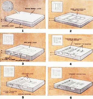
 1. Raw material for a solid-state microcircuit, a basic silicon chip-one of many
in a semiconductor wafer. It consists of a p-type substrate, an epitaxial n-type
layer and a thin passivating layer of silicon dioxide, to protect it against contamination.
2. A solid-state integrated circuit, like one made by the thin-film process, still
consists of separate elements, though now each is made by the same process and out
of identical materials. But each element still needs its own "living room" and must
be isolated from other components on the same chip. The wafer is masked to leave
protected islands. The protecting oxide layer around these islands is etched off
and p-type material is diffused into the resulting channels deep enough to meet
the p-type material of the substrate and isolate the n-type islands. 1. Raw material for a solid-state microcircuit, a basic silicon chip-one of many
in a semiconductor wafer. It consists of a p-type substrate, an epitaxial n-type
layer and a thin passivating layer of silicon dioxide, to protect it against contamination.
2. A solid-state integrated circuit, like one made by the thin-film process, still
consists of separate elements, though now each is made by the same process and out
of identical materials. But each element still needs its own "living room" and must
be isolated from other components on the same chip. The wafer is masked to leave
protected islands. The protecting oxide layer around these islands is etched off
and p-type material is diffused into the resulting channels deep enough to meet
the p-type material of the substrate and isolate the n-type islands.
3. A new oxide layer is grown over the diffused area for greater protection,
and 4. the wafer again masked and "windows" etched through the layer over the islands,
so that p-type material can be diffused into precisely located regions to form resistors,
bases for transistors and the anodes of di-odes and capacitors.
(To understand why a simple p-layer can isolate two islands, look at the left
two such islands in the foregoing pictures. There are two semiconductor islands,
an n-p junction formed by the left island and the substrate and a p-n junction between
the substrate and the middle island. The two junctions form a back-to-back-connected
diode effect, so no matter what the polarity of the two islands, the very high resistance
of a back-biased diode is always between them. Every back-biased diode is a capacitor,
so there is parasitic capacitive coupling between them as well. This must be taken
into account in high-frequency circuit design, and of course is used intentionally
for solid-state capacitors.)
5. Next step is to grow a new oxide insulating layer over the newly formed p-type
transistor base and resistor areas and 6. large windows are again etched for emitters.
These are of heavily doped material with very low resistivity. Consequently, emitter
material is often used for interconnecting leads between various parts of semiconductor
circuits, and occasionally for low-value resistors.
7. All that now remains is to connect our "components" together in a circuit.
Tiny windows are etched through to the point where leads are to be connected. A
thin coating of metal is then evaporated over the entire wafer, so that it penetrates
through the openings to make perfect contacts. Another photo-masking step 8. and
an etch removes the metal, leaving only the required interconnecting pattern atop
the oxide. The masking also provides islands around the edges for connection to
external circuits.
Now the wafer 9. is carefully scribed and broken up into individual chips, each
one containing a complete circuit. The chips are then mounted on headers. A typical
mounting is a transistor type case (TO-5) but flat packages are also made. After
each chip has been mounted, a metal cap is welded over the assembly to seal it hermetically.
Since the number of parts in an integrated circuit has little effect on material
costs, two or more transistors may be made instead of one, without increasing the
cost noticeably. This is another advantage, since engineers are not impelled by
economic considerations to design circuits with the minimum number of parts.
Integrated circuits also reduce inventory costs, shipping and transportation
expense, and the various costs connected with purchasing at every manufacturing
level.
These advantages, added to those of miniaturization and reliability, clearly
indicate that microcircuitry is destined to take over in many areas of electronic
manufacturing.
* Manager, Technical Information Center, Motorola Semiconductor Products.
Posted January 9, 2023
|