|
January 1960 Radio-Electronics
 [Table of Contents] [Table of Contents]
Wax nostalgic about and learn from the history of early electronics.
See articles from Radio-Electronics,
published 1930-1988. All copyrights hereby acknowledged.
|
Although the Hall effect
had been known for 80 years when this article appeared in Radio-Electronics
magazine in 1960, it was not until research in semiconductor compounds during that
same era generated substantial enough voltage potentials for detection and use by
circuits of the day that
Hall effect sensors became useable in mass production.
Indium arsenide (InAs)
and indium antimonide
(InSb) are two of the early examples. A single Hall effect sensor in 1960 would
set you back around $25 - that's
$253 in today's money... ouch! Hall effect sensors in small quantities can be
bought now from Digi-Key for $2 and change. Modern Hall effect sensors are still
made with InAs and InSb, along with gallium arsenide (GaAs), indium phosphide
(InP), and even
graphene. There is obviously
something special about indium (In)
that makes it the ideal base metal for Hall sensors. All the elements involved are
in the p-block
group of the periodic table.
Something New in Semiconductors
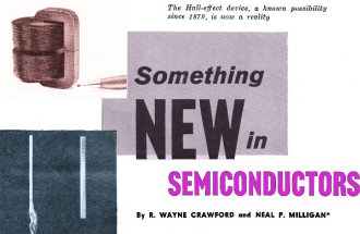
The Hall-effect device, a known possibility since 1879, is now
a reality
By R. Wayne Crawford and Neal P. Milligan*
1879, E. H. Hall, a physicist at Harvard University, discovered an effect which
has become known as the Hall effect and today is the basis for a new series of semiconductor
devices. Hall determined that, when a conductor through which current is flowing
is placed in a magnetic field perpendicular to the conductor, a voltage is developed
across it.
For a clearer picture of this action, take a look at Fig. 1. When there is no
magnetic field, the electrons flow through the conducting slab in a straight line
(labeled control current) and there is no voltage difference across the slab. If
a magnetic field is applied, the electrons are deflected toward the side as shown,
leaving a surplus of positive charges on the opposite side of the slab. This creates
a voltage difference across the slab, known as the Hall voltage. This voltage is
proportional to the product of the current passing through the conductor and the
magnetic flux density (magnetic lines per unit area). The magnitude of the Hall
voltage for a given current and magnetic field depends on the ease with which electrons
can move through the material, so the ease of movement becomes a figure of merit
for the material and is called "charge-carrier mobility." The higher the charge-carrier
mobility, the higher the Hall voltage for a given magnetic field and control current.
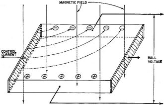
Fig. 1 - Basic action of a Hall-effect device. The electrons
supplied by the control circuit are deflected by the magnetic field to one side
of the conducting slab. This leaves an excess of positive charges on the opposite
side, thereby causing a voltage known as the Hall voltage, across the slab.
Until recently, no known material had a charge-carrier mobility high enough to
allow Hall voltages great enough to be of practical use. But the development of
intermetallic compounds - indium arsenide and indium antimonide - has made Hall-effect
devices practical. Such Hall-effect devices are now commercially available.
For most applications, a magnetic circuit produces the magnetic field needed
to operate the Hall-effect device. A sketch of such a circuit is shown in Fig. 2.
The input currents passing through the coils create a magnetic field. As many coils
as the physical configuration of the core will allow can be used. The top head photo
shows a typical magnetic circuit using two center-tapped coils. The total magnetic
field is equal to the sum of the magnetic fields generated lily each coil. To reduce
the number of coil turns needed to produce a given magnetic field, the gap in the
core is made very small. The gap can be made small since the Hall-effect device
is very thin, as shown in the bottom head photo.
The Hall-effect device is truly a low-level device in all respects. The maximum
control current, when operated in free air, is approximately 500 ma.
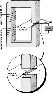
Fig. 2 - Typical 2-coil magnetic circuit. The iron core concentrates
the magnetic field on the Hall-effect device.
The output Hall voltage is in the order of hundreds of millivolts. The input
and output impedances are on the order of 1 ohm. To obtain such low-level impedances
with vacuum tubes or transistors requires complex circuits. The Hall-effect device
is filling a real need in the electronics field by providing a low-impedance circuit
element. It also has the property of being able to function equally well with either DC or AC inputs.
A typical Hall-effect device multiplying circuit is shown in Fig, 3. The magnetic
field generated by the coil is proportional to the current flowing in the coil.
The output voltage is, therefore, proportional to the product of the magnetic circuit
current and the control current. If more than one coil is used in the magnetic circuit
and if the control current is held constant, the output voltage is proportional
to the sum or difference (depending upon their relative polarity) of the input currents.
By appropriate switching, a single Hall-effect device and magnetic circuit can perform
all of these functions.
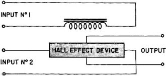
Fig. 3 - An electronic multiplier circuit. The output voltage
is proportional to the product of the two inputs.
The Hall-effect devices described here are new, even though the principle has
been known many years. They have been manufactured in the United States less than
a year. As were the first transistors, Hall-effect devices are relatively expensive
today - about $25 each in lots of one. However, it is reasonable to assume that
as with transistors, their cost will drop in a short time.
The potential applications of these devices are almost limitless. They may be
used in computer circuits to add, subtract and multiply. With an amplifier, they
have been used to measure the earth's magnetic field. They are being used in both AC and DC power meters. They may be used to match a high impedance to a low impedance
and provide isolation at the same time. These devices and the associated magnetic
circuit may be considered as a DC transformer, since they provide transformer action
even with direct currents.
These new semiconductor devices present an entirely new concept in the field
of circuitry and will play an important role in the design of new electronic equipment.
* Technical consultant, and manager of Applications Div., respectively, Ohio
Semiconductors.
Posted January 25, 2023
|