|
May 1958 Radio-Electronics
 [Table
of Contents] [Table
of Contents]
Wax nostalgic about and learn from the history of early electronics.
See articles from Radio-Electronics,
published 1930-1988. All copyrights hereby acknowledged.
|
Did I ever tell the story about
a manager I had at a major defense electronics firm who thought he could make an
NPN transistor by wiring two diodes in series with the anodes tied together? He
reasoned that since a bipolar junction transistor consisted of three alternating
layers of n-type and p-type silicon, the device could be affected per his scheme.
That was in the mid 1980s when I was still a technician (working diligently
on my BSEE degree at night). Needless to say the engineers who worked under
him were not too impressed with the guy's technical prowess (nor his managerial
prowess, as I remember it). I didn't consider myself qualified at the time
to judge him one way or the other, so the fact that he was a good guy made him OK
in my book. This article from the year I was born reports on the advancements during
the first decade of the transistor era. It was just before Christmas of 1948 that
Mssrs. Brattain, Bardeen, and Shockley announced to the world their universe-changing
invention.
Ten Years of Transistors
Transistors have been with us for a decade and much has happened in that
brief period, Here is a condensed history of the transistor from its inception in
1948.
By R. M. Ryder*
 Just 10 years ago - on June 30, 1948 - Bell
Telephone Laboratories announced the invention of a semiconductor amplifier and
coined for it the name transistor. This invention has been termed one of the most
significant milestones in the history of electronics. The transistor in various
forms, some of them barely as large as a shoelace tip, is capable of doing most
of the things electron tubes can do, and many other things as well, most of them
on amazingly small amounts of power. Just 10 years ago - on June 30, 1948 - Bell
Telephone Laboratories announced the invention of a semiconductor amplifier and
coined for it the name transistor. This invention has been termed one of the most
significant milestones in the history of electronics. The transistor in various
forms, some of them barely as large as a shoelace tip, is capable of doing most
of the things electron tubes can do, and many other things as well, most of them
on amazingly small amounts of power.
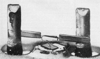
The first form of this device consisted of a tiny wafer of germanium on which
were placed two closely spaced point contacts, one controlling the flow of current
in the other. It was called a point-contact transistor. Its invention, by John Bardeen
and Walter H. Brattain, stimulated a tremendous upsurge in semiconductor research,
which has continued without letup to the present. The upsurge has been continually
stimulated over the years by new developments and constantly improving techniques,
and there is no evidence that this interest will wane in the foreseeable future.
The transistor has a long history of semiconductor research behind it. As far
back as 1833, Michael Faraday observed that silver sulfide had a negative temperature
coefficient of resistance. This characteristic set it apart from other conductors
(metals) whose resistance increased with increasing temperature. By 1855, four of
the fundamental properties of semiconductors- negative temperature coefficient
of resistance, rectification, photoconductivity and photoelectromotive force - had
been observed.
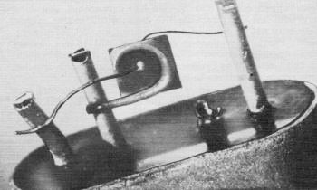
Internal structure of a single-diffused germanium transistor.
Bent wires from posts lead to emitter layer and base contact on surface of crystal.
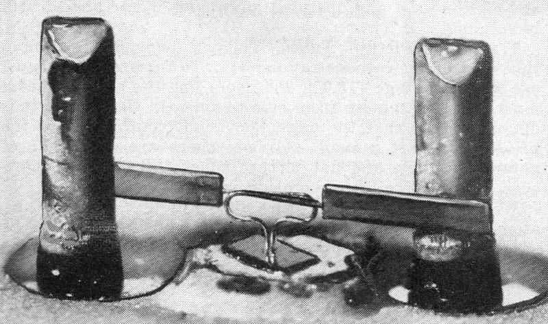
Heart of intrinsic-barrier transistor as seen through a microscope.
Tiny electrical sandwich in center of photo contains positive, negative, neutral
and positive layers and holds two tiny dots of indium, to which input and output
electrodes are connected.
A great body of knowledge on semiconductor materials was built up and contributed
greatly to the final success of the transistor. Research workers were concerned
with both surface and body phenomena. With respect to surfaces, it was postulated
that a space-charge layer should exist at the surface of a semiconductor. Experiments
were set up to verify the existence of this layer, and these experiments led to
the birth of the point-contact transistor.
The junction transistor
Following rapidly on the heels of this development was the announcement of the
junction transistor in 1951 by William Shockley of Bell Laboratories.
This radically new form of the device was in many ways more effective than the
original point-contact type, being freer from noise and more efficient. Most striking
is that it was predicted theoretically by Shockley more than 3 years before it was
demonstrated.
Because of space limitations, it is not possible to review all of the advantages
of transistors. However, the basic abilities such as low power consumption, small
size, and reliability have been widely publicized and are well known.
The junction transistor consists essentially of a sandwich of semiconductor materials
into which controlled amounts of impurities have been introduced to provide specific
characteristics. Germanium has four valence electrons in its outer shell and, when
formed into a single crystal, there are no excess electrons or holes to conduct
electricity. However, if a small amount of an element having five valence electrons
is added to the germanium, excess electrons will be present, and n-type germanium
results. Two such elements are antimony and arsenic. If the added element has only
three valence electrons, excess holes will exist, forming p-type germanium. Elements
in this class are typified by gallium and indium. The transistor sandwich then consists
of a layer of n-type germanium, for example, with p-type on each side. The center
layer of this sandwich is very thin.
Several techniques have been developed for creating this alternate n-p-n or p-n-p
type of construction in a single crystal. For example, if a single crystal is being
grown of n-type material and the melt is doped to make it p-type, a thin layer will
grow. If the melt is immediately doped to again make it n-type, a sandwich will
be formed with a very thin center layer. This is called a grown-junction transistor.
Steps involved in the fabrication of a germanium grown junction transistor1
are shown in Fig. 1.
Another technique is to alloy opposite faces of a thin wafer of p-type germanium
with some such material as arsenic to make the faces n-type2. This is
called an alloy junction transistor is indicated in Fig. 2. Regardless of the
method of fabrication, these junction transistors operate on essentially the same
basic principles.
A closely related device is the photo-transistor3. This was an entirely
new type of electric eye - much smaller and sturdier than existing photoelectric
devices. It is essentially a transistor controlled by light rather than by electric
current.
This transistor is employed extensively in the "card translator," a system used
in telephone exchanges for automatic routing in toll dialing.
Zone refining
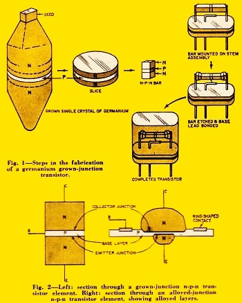
Fig. 1 - Steps in the fabrication of a germanium grown-junction
transistor.
Fig. 2 - Left: section through a grown-junction n-p-n transistor
element. Right: section through an alloyed-junction n-p-n transistor element, showing
alloyed layers.
The materials needed for semiconductor device research are among the purest and
most perfect known to science. Large single crystals having impurities of about
1 part in 10,000,000 are routinely required. These small impurities must also be
controlled to within a few percent. The major breakthrough which made such material
easily achievable was the "zone-refining" technique, announced by W. G. Pfann of
Bell Laboratories in 1954.
In zone refining, a molten zone is swept through an ingot of the semiconductor
material, such as silicon or germanium, sweeping impurities to one end of the bar.
By repeated sweeps, undesirable impurities can be reduced to less than 1 part in
1,000,000,000. The technique takes advantage of the fact that the solubility of
impurities in liquid semiconductor material is different from the solubility in
the solid.
The importance of the purification process is apparent when you realize that
active impurities of as little as 1 part in 1,000,000,000 can affect transistor
operation. It is essential that the material be as pure as possible to begin with,
so that the desirable properties can be obtained by introducing controlled amounts
of the desired impurity.
Throughout the semiconductor development process, efforts were made to improve
the frequency range of transistors, both as oscillators and as amplifiers. One approach
was to reduce the thickness of the center layer of the sandwich, but certain limitations
were encountered. A major step in overcoming these limitations was achieved with
the invention of the tetrode transistor4. By 1955, this transistor had
been developed to the point where it could be made to oscillate at more than 1,000
mc, thus breaking into the microwave region for the first time with solid-state
amplifiers.
Operation at such high frequencies was achieved by adding a fourth electrode
to the basic junction transistor, plus other refinements. This fourth electrode
permitted the center layer of the transistor to be biased in a way that reduced
its effective thickness. This, combined with an actual reduction in thickeness
to less than 0.2 mil, provided operation at ultra high frequencies.
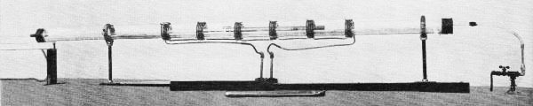
Completely uncontaminated metals can be produced by this zone-melting
apparatus.
The role played by minute quantities of impurities in controlling the properties
of metals can then be determined.
The field-effect transistor
The foregoing discussion has revolved around a particular type of transistor
action, namely the injection of charge carriers by a p-n type junction into a thin
slice of semiconductor and their collection by another junction. It is also possible
to get amplification by other means, as in the field-effect transistor, where a
transverse electric field controls the flow of current. A number of such "unipolar"
transistors were described by Shockley in 19525. This type of operation
may have important advantages; in particular, high input impedance of the order
of 10 megohms and the possibility of very high frequency response. Very similar
in concept are the "analog" transistor and the spacistor.
A field-effect transistor using an external "gate" is shown schematically in
Fig. 3, while Fig. 4 shows a field-effect transistor using a p-n junction
to produce a capacitor "gate" within the body of the semiconductor.
Another significant step in high-power and high-frequency operation was the introduction
of the p-n-i-p, or "intrinsic-barrier" transistor.6 This transistor is
in essence a club sandwich, in which a layer of comparatively pure material is interposed
between two of the layers of a conventional transistor. This layer permits closer
control of the stream of charge carriers, isolates input and output areas and reduces
the stored energy to make functioning at higher frequencies possible. The increased
separation of input and output areas also permits operation at higher voltages than
possible with earlier transistors. The intrinsic layer might be compared very roughly
with the screen grid in a vacuum tube.
Intrinsic barrier type transistors can provide uniform amplification over bands
of hundreds of megacycles, and theoretically units can be made which will oscillate
at 3,000 mc. They can also be designed to produce some 3 to 10 times more power
than earlier junction transistors at high frequencies.
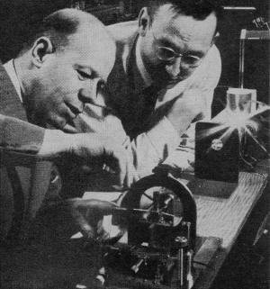
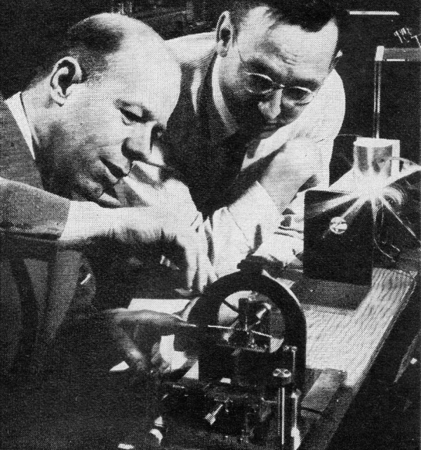
Testing the alignment of phototransistors used to "read" information
stored by electronic computers, are Dr. J. N. Shive (left), who developed the phototransistor
and Dr. R. M. Ryder, both of Bell telephone Laboratories.
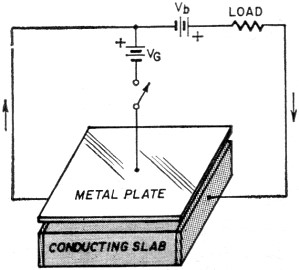
Fig. 3 - Schematic representation of a field-effect transistor
in a circuit designed to illustrate how current through the slab can be controlled
by applying a voltage to the metal plate.
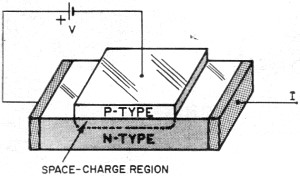
Fig. 4 - A field-effect transistor using a p-n junction
to produce a "capacitor" within the body of the semiconductor. A voltage that is
applied between the p- and n-type material causes a penetration of space charge,
creating a region within the body of the n-type material that will not contribute
to current flow through the semiconductor.
The surface-barrier transistor7 represented another step toward high-frequency
operation. In this unit, both sides of a thin wafer of germanium are electrolytically
etched away until only an extremely thin layer remains. Electrodes are then deposited
electrolytically. Because of the very thin base layer, high-frequency operation
is possible. This transistor has since been further improved by incorporating a
diffused base and by closely controlled alloying of the junctions.
The diffusion technique
In 1954, Bell Laboratories announced a development which has proved to be a major
breakthrough in transistor technology - the diffusion technique. Diffusion is a
process by which minute amounts of impurities are introduced into a material in
a controlled manner. As mentioned previously, one of the limitations in extending
the operation of conventional junction transistors to ever higher and higher frequencies
is the difficulty of reducing the thickness of the center layer of the transistor
sandwich. By introducing impurities in a controlled manner by the diffusion process,
this layer can be made as thin as 30/1,000,000 inch.
The diffusion technique8,9 can be used for other semiconductor devices
as well. Among these devices is the Bell solar battery.10 This battery
consists of a thin wafer cut from a single crystal of n-type silicon into which
a small amount of boron has been diffused to produce a thin layer of p-type silicon.
When illuminated, this cell produces electricity. In direct sunlight, its conversion
efficiency may run as high as 11 %.
At present, it appears that the diffusion technique will achieve widespread recognition
as a reliable, controllable process for making transistors and many other semiconductor
devices. Enough information has been obtained on this process to make it adaptable
to mass-production operations. Units have been fabricated which will oscillate and
amplify at well over 1,000 mc, and the frequency barriers are continually being
forced higher and higher.
The "drift transistor" emphasizes another feature which has importance for high-frequency
transistors.11 By control of the distribution of impurities in the thin
central layer, one can obtain a "built-in" electrical field which speeds up the
electron stream and thereby makes the transistor somewhat faster. Experimentally,
the easiest way to achieve an appropriate structure is by diffusing the base as
just mentioned above. Typically, the frequency response improves 10 or 100 times
by making the base layer thinner while the built-in field gives a further improvement
of the order of 1.5-4 times.
Last year a new device was announced which combines high-frequency operation
with high-power output to an extent not previously attained. This new transistor
can provide an output of better than 5 watts at 10 mc, either as an oscillator or
an amplifier. It has alpha-cutoff frequency of about 100 mc and has produced an
output of better than 1 watt at this frequency.
To achieve the combination of high power and high frequency required extensive
research and the utilization of many different techniques. The unit employs the
basic p-n-i-p type of construction and so takes advantage of the intrinsic-layer
idea. Silicon is employed to permit operation at higher temperatures and thus allow
greater heat dissipation. Diffusion techniques are used to form the emitter and
collector regions. And the electrode areas themselves are kept as small as possible
consistent with the desired power-handling capacity. Thus, by combining a number
of techniques, both frequency and power barriers have been lifted.
Electronic computing machines are one of the newest fields that transistors are
expected to dominate because of their size, power, speed and reliability. Closely
related is the field of automatic telephone switching, which now uses electromechanical
switches such as relays but which is expected to go increasingly electronic in coming
years. A prominent new device for use here is expected to be the p-n-p-n diode,
a four-region transistor switch, invented by Shockley. As now realized in diffusion
techniques in silicon, the device in the off condition has a resistance of 100 megohms.
When switched on either by a pulse or by a high voltage, its on resistance is only
about 2 ohms, with a less than 1-volt sustaining voltage. The device can be switched
between these conditions at megacycle rates if necessary.
New fabricating processes
A major problem in fabricating transistors, particularly those intended for high-frequency
operation, is attaching leads to the semiconductor material. A significant advance
in this field is the development of the thermocompression bonding technique at Bell
Laboratories. In this technique, the leads are attached by a combination of temperature,
pressure and time. One method that works very satisfactorily in he laboratory is
to force the lead against the semiconductor surface with a heated wedge-shaped tool.
Neither the temperature nor the pressure is great enough to damage the semiconductor
surface nor to introduce any impurities, and the time can be kept short enough to
permit rapid assembly.
Advantages of this method over soldering or welding are many. There is less danger
of contamination; leads can be attached to very small areas - particularly useful
in high-frequency transistors - and the bond between the lead and the semiconductor
is stronger than the lead itself.
Although today's practical transistors all use germanium or silicon, at least
passing mention must be made of a new family of materials called intermetallic semiconductors.
Silicon and germanium are in Group IV of the periodic chart; that is, they each
contain four valence electrons in the outer ring. Compounds formed by taking elements
from Group III (three valence electrons) and Group V (five valence electrons) will
have an "average" of four valence electrons, and thus may exhibit characteristics
similar to the materials now used.
A great deal of exploratory work is being carried out in laboratories both in
this country and abroad to determine the characteristics of these intermetallic
compounds. Particularly active in his field is H. Welker, in Germany. Results have
been very encouraging - it appears that these materials may be useful for producing
more versatile transistors and other devices. In fact, intermetallic diodes are
now on the market. Notable among the compounds under investigation are indium antimonide,
gallium arsenide and indium phosphide.
More complex compounds having an average of four valence electrons in the outer
ring are also being investigated, and it is reasonable to expect that within a few
years materials will be available which are superior in specific areas to either
germanium or silicon.
Important areas of exploration, at present, are in the areas of surface phenomena
and external contamination. To produce reliable transistors having the desired characteristics
without excessive rejects requires careful control of all the steps in the manufacturing
process, with particular emphasis on avoiding contamination of any kind. Past efforts
in this direction have paid off handsomely. Work is also under way to increase power
and frequency capabilities of transistors to approach more closely the performance
now available from electron tubes.
An attempt has been made here to touch on the highlights of the last 10 years
of transistor development. Many important contributions and contributors have of
necessity been omitted for lack of space. It is important to emphasize that in this
field, as well as any other scientific endeavor, notable advances are the result
of the combined efforts of a number of scientists striving to unlock the secrets
of nature.
*Bell Telephone Laboratories.
1 W. Shockley, M. Sparks and G. K. Teal, "P-n Junction Transistors"; Physical
Review, Vol. 83, pp. 151-62, July 1, 1951.
2 John S. Saby, "Fused Impurity P-n-p Junction Transistors"; Proceedings of the
IRE, Vol. 40, P. 1358, November, 1952.
33 J. H. Shive, "The Phototransistor"; The Transistor: Selected Reference Material
on Characteristics and Applications, Bell Telephone Laboratories, Inc., New York,
1951 (prepared for Western Electric Co.), p. 115.
4 R. L. Wallace, Jr., L. G. Schimpf and El Dickten, "A Junction Transistor
Tetrode for High-Frequency Use"; Proceedings of the IRE, Vol. 40, p. 1395, November
1952.
5 W. Shockley, "A Unipolar 'Field-Effect' Transistor"; Proceedings of the IRE,
Vol. 40, p. 1377, November, 1952.
6 J. M. Early, "P-n-i-p and N-p-i-n Junction Transistor Triodes" ; Bell System
Technical Journal, Vol. 33, p. 517, May, 1954.
7 W. E. Bradley, et al, Proceedings of the IRE, December, 1953.
8 M. Tanenbaum, D. E. Thomas and C. A. Lee, "Diffused Emitters and Bases for
Silicon and Germanium Transistors"; Bell System Technical Journal, January, 1956.
9 C. S. Fuller and J. A. Ditzenberger, "Diffusion of Donor and Acceptor Elements
in Silicon"; Journal of Applied Physics, Vol. 27, May, 1956.
10 D. M. Chapin, C. S. Fuller and G. L. Pearson, "The Bell Solar Battery"; Bell
Laboratories Record, July, 1955.
11 H. Kromer, "Theory of the Germanium Rectifier and the Transistor"; Zeitschrift
Physik, Vol. 134, pp. 435-50, March 25, 1953.
The Author
Robert M. Ryder was born March 8, 1915, in Yonkers, N. Y. He graduated from Yale
in 1937, receiving a Bachelor of Science degree in physics. He obtained a PhD degree,
also from Yale, in 1940.
In July, 1940, he become a member of the technical staff of Bell Labs, working
on microwave amplifier circuits. During World War II, he contributed to Bell Labs'
research on the signal-to-noise performance of radars. In 1945, he joined the Electronic
Development Department to work on microwave oscillators and amplifier tubes for
radar and radio relay applications. He is currently a transistor development engineer,
particularly interested in transistor development for high-frequency and other transmission
applications.
In 1957, Dr. Ryder received an award from the Institute of Radio Engineers "for
contributions to the development of microwave tubes and applications of transistors."
He is a member of the American Association for the Development of Science, Sigma
Xi and the Yale Engineering Society.
Posted October 13, 2022
(updated from original post
on 10/16/2014)
|