|
February 1969 Radio-Electronics
 [Table of Contents] [Table of Contents]
Wax nostalgic about and learn from the history of early electronics.
See articles from Radio-Electronics,
published 1930-1988. All copyrights hereby acknowledged.
|
By the time this "Test
Transistors Fast" article appeared in a 1969 issue of Radio-Electronics
magazine, the use of vacuum tubes in new designs had been relegated to the
domain of hobby and specialized circuits. Very high power and frequency
applications were still waiting for semiconductors capable of servicing such
equipment, but the electronics industry, particularly the domestic consumer
world, used transistors and what was available in the form of integrated
circuits. While designers had already been using transistors for a decade or
more, many of the aforementioned hobbyists and electronics repair servicemen
were still getting accustomed to the newfangled technology and welcomed the
publishing of these kinds of topics. In 1969, the only thing I knew about
transistors was that they must have somehow been associated with the "transistor
radio" I carried in my jacket pocket. It was too small to contain any of those
glowing tubes we still had in our household TV set and tabletop radios (and in
the dashboard of our family's 1960 Rambler auto for that matter), so surely
there was a difference. If you are new to transistors because of just now
getting into the field of electronics, then even though written half a century
ago, the information is still relevant.
Test Transistors Fast - ABC's of Transistors
Transistor curves
Learn how ohmmeters and transistor testers show solid-state faults. Study new
age and horizontal circuits
By Sylvania Technical Staff
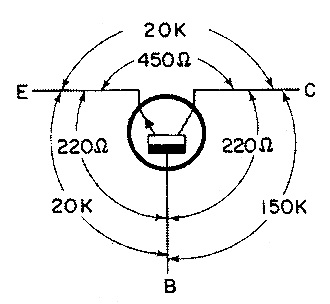
Ohmmeter tests will weed out definitely defective transistors. Since a transistor
can be considered as two diodes connected back-to-back, the equivalent circuit (Fig.
1) is a guide to making simple resistance tests. For example, you should find a
reasonably high front-to-back ratio between emitter and base, as well as between
collector and base.
If you find a low resistance when the negative ohmmeter lead is connected to
the emitter and the positive lead to the base, the transistor is an npn type. A
high resistance here indicates a pnp type.
You may or may not measure a substantial front-to-back ratio from emitter to
collector, even if the transistor is in good condition. A few transistors are symmetrical,
meaning that the emitter and collector junctions have identical characteristics.
For such devices the front-to-back ratio from emitter to collector is unity. On
the other hand, most transistors are unsymmetrical, and you will measure a definite
front-to-back ratio from emitter to collector although this ratio is usually lower
than the other two ratios. Ohmmeter measurements on a "good" transistor selected
at random are noted in Fig. 1.
Junction Resistances
Typical resistance measurements on a "good" NPN transistor.
Transistor current designations between junctions.
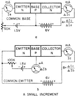
NPN and PNP measurement setups.
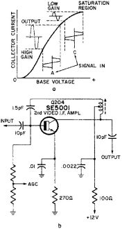
Linear and nonlinear operating regions of transistor.
Typical gain bias voltages in audio circuit.
Transistorized AGC circuit.
CRT deflection coil driver circuit.
Example horizontal deflection generator circuit.
Audio amplifier circuit example.
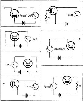
Simple transistor testers are basically ohmmeters. A common follow-up test is
to measure junction back resistances in terms of current flow. Nearly all testers
provide an ICBO test, which measures leakage current. It applies a moderate
reverse voltage between collector and base with the emitter open, as in Fig. 2.
A microammeter in the collector circuit indicates whether the back resistance of
the collector junction is acceptably high. Manufacturers list ICBO.
An ICES test is made the same way, except that the emitter is shorted
to the base. The ICES current flow is normally somewhat greater than
ICBO current flow. Transistors are customarily rated for ICES
as well as ICBO. Simple transistor testers seldom provide an ICES
test.
An IECS test is basically the same as an ICES test, except
that emitter and collector terminals are reversed. The reverse emitter-junction
current is measured with the collector shorted to base. In a truly symmetrical transistor,
IECS and ICES readings are normally the same.
Many transistor testers do provide an ICEO test. An ICEO
reading is normally greater than an ICBO reading because the reverse
current is increased by emitter-base junction action. This test, as well as the
foregoing tests, are provided by instruments with maximum flexibility for de tests.
Alpha and Beta
A more critical test of a transistor is to measure its alpha or beta (see Fig.
3). Basically, this is a measurement of transfer resistance. As shown in Fig. 3-a,
the emitter is forward-biased, and the collector is reverse-biased. A forward emitter-bias
lowers the emitter junction resistance, which is transferred by lattice action as
a lowering of the collector junction resistance. Alpha is defined as the ratio of
collector-to-emitter current. Beta is defined as the ratio of collector-to-base
current of the transistor.
The simple ratio of input to output currents gives the DC (static) alpha or beta
of a transistor. This is a test that simulates large-signal operation of a transistor,
where the input signal drives the transistor over a large excursion of its characteristics.
On the other hand, transistors are commonly rated for small-signal operation, and
published values of alpha and beta must be checked by a slightly modified procedure.
Small signal alpha and beta
To check small-signal alpha and beta, input current is set to an operating value
specified by the transistor manufacturer. This establishes an operating point at
a median in the characteristics, as might be used for class-A amplification. Then,
input current is increased by a small amount. The corresponding change in collector
current is noted. The small-signal alpha or beta is then given by the ratio of input-current
change to output-current change. Alpha and beta are simply related to each other,
as in Fig. 3.
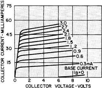
The DC alpha or beta will not be the same as the small-signal alpha or beta because
the transfer resistance of many transistors is nonlinear (Fig. 4). Note that a base-current
change from 0 to 0.3 ma produces a much larger collector-current change than a base-current
change from 0.9 to 1.2 ma. Hence, this transistor will measure a larger DC beta
than its small-signal beta.
Transistor Circuit Applications
Automatic gain control: The age system develops a DC voltage
in a tv receiver that has a direct relationship to signal strength. This voltage
controls the gain of RF and video i.f. stages to limit picture variations due to
changes in signal strength. For the most accurate age, the system is referenced
to the portion of the signal which does not vary as a function of video information.
These systems ere keyed or gated and referenced to the signal during horizontal
sync pulse time, which represents 100% carrier power of the input signal. To reference
at any other time could produce an agc voltage that would vary as the picture content
varied; i.e., more age voltage on black scenes and less age voltage on white scenes,
etc. Also the effects of noise on the age system should be minimized.
In most receivers, the chassis operates at maximum sensitivity when no signal
is being received. When a signal is received, a voltage is developed that is proportional
to the strength of the incoming signal. This agc voltage is used to control receiver
gain. In a conventional tube-type tuner, a negative voltage controls tuner gain.
Deviation occurs when gain reduction is applied to the video i.f. of solid-state
sets. Here, gain reduction is handled by increasing the forward bias, which increases
collector current in the transistor. Since a positive-going voltage is required
to increase the npn transistor's forward bias, the negative age voltage is used
to control an agc amplifier stage which. in turn, produces a positive voltage change
at the base of the i.f. transistor controlled by agc. When an incoming signal becomes
stronger, the negative age voltage increases and increases in the positive voltage
on the base of the i.f. transistors (reducing i.f. gain).
The basic principle involved in using an increase in forward bias to reduce amplifier
gain is shown in Fig. 5.
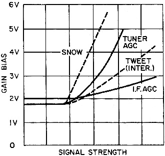
In some sets special circuits are used so that above a certain level, the i.f.
and tuner receive different bias voltage ratios. The signal compared to bias for
both i.f. and tuner is shown in Fig. 6.
Different voltages are used for the tuner and i.f. to keep the tuner in its best
response range. The graph also shows noise and tweet extremes in tuner agc levels.
Signal strength is determined by "measuring" the horizontal sync pulse amplitude.
This is the conventional means with keyed age systems. The average video level is
not used since scene changes would appear as signal strength changes.
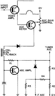
Composite video is taken from the collector of the first video amplifier. The
signal at this point is positive sync. This signal is applied to the base of the
age keyer. Since the age keyer is an npn transistor, the positive sync tends to
make it conduct (see Fig. 7).
The keyer has the agc control in the emitter leg, which changes the gain of the
keyer.
The agc keyer has no collector supply except for a positive pulse during the
horizontal sync time. A diode connected in series with this pulse prevents the keyer
from conducting except when the positive pulse is present. The agc coil also has
a negative excursion which would forward bias the keyer's collector and destroy
the transistor.
The positive keying pulse is supplied from a coil on the fly back transformer,
the return leg of the agc amplifier. The amount of current drawn from the agc amplifier
base circuit is proportional to the amount which the keyer is conducting which,
in turn, depends on the sync pulse amplitude.
A capacitor in the base circuit of the agc amplifier charges to some value through
R1. The higher the sync pulse amplitude, the greater the drain on the capacitor's
charge. The less the charge on the capacitor, the less the agc amplifier conducts.
We then have a system which causes the agc amplifier to conduct more as the signal
weakens and conduct less as the signal increases. Consequently, under maximum signal
conditions the agc amplifier is driven toward cutoff and the collector voltage is
at maximum. Maximum positive agc causes amplifier gain.
The collector voltage is fed directly to the tuner age line. Under maximum signal
conditions, the i.f. age voltage is divided first by R2 and R3 and then by R4 and
R5. Since conduction through R3 and R4 is light, the reverse voltage difference
across the diode is large and it remains non-conducting.
As the signal weakens, the agc amplifier begins to conduct, which causes the
reverse voltage differential on the diode to decrease. At some point, the diode
conducts and places almost the same age voltage on the i.f. as the tuner.
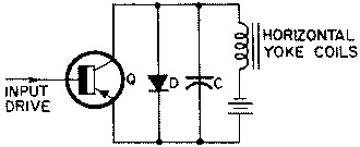
Horizontal Deflection
The horizontal deflection requirements for a TV set call for a magnetic field
capable of linearly deflecting the beam across the tube face and returning it to
a starting point 15,750 times per second. An equivalent form of deflection circuit
is in Fig. 8.
The transistor acts as a switch across the entire coil and power supply network.
If the transistor is switched on, the yoke coil's current increases at about a linear
rate. When a set time interval elapses the transistor is turned off. The inductive
kick from the coil is impressed on the transistor diode and capacitor C. The coils
and capacitor form a tank circuit and tend to oscillate or ring. The diode acts
as a short or closed circuit on the opposite polarity of each "ring" cycle. By proper
timing of transistor and diode switching, a sawtooth current passes through the
coils. This current averages out to be near zero, provides circuit efficiency, and
removes the need of beam decentering. Beam decentering means the need for its starting
point to always be at one extreme side of the screen.
After the transistor is switched off and coil energy is transferred from the
capacitor back to the coil, polarity reversal occurs and the damping diode conducts.
The current is now flowing in the coils in the reverse direction and approaches
zero. When zero is reached the transistor is again turned on, starting another cycle.
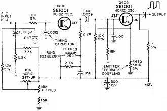
Horizontal Oscillator
The horizontal oscillator circuit in the Sylvania A02 chassis (Fig. 9) is an
emitter coupled, two-stage multivibrator. Regenerative feedback voltage between
stages is developed across the common emitter resistor.
When Q400 is at cut-off, collector voltage is about equal to battery voltage.
This positive voltage is coupled to Q402 by C416, placing a forward positive voltage
on the base of Q402. Q402 then goes to saturation and minimum collector voltage
results. The positive voltage developed across R430 maintains a reverse bias on
Q400, emitter to base. As the more negative base voltage of Q400 is neutralized
(depending on the horizontal hold control setting) by the plus 12-volt supply voltage,
the transistor goes back into conduction. Its collector voltage drops, applying
a negative voltage to the base of Q402 and driving it to cut-off. This results in
loss of emitter voltage on Q400, which is again biased off and the cycle repeats
itself.
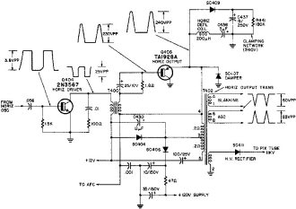
Horizontal output circuit
The horizontal oscillator input (in a Sylvania A02 chassis) to driver stage Q404
is approximately a square wave at about 3.8 volts peak-to-peak (see Fig. 10). It
is amplified by the driver stage to a 25-volt peak-to-peak pulse. It is then applied
to T400 to drive the final output Q406. This transistor normally conducts at saturation,
and when the driver pulse is applied is cut-off almost instantaneously. This is
a positive pulse from T400 and reverse biases the emitter base junction of Q406.
When Q406 stops conducting, the heavy B-plus current flowing through the transistor,
through T402 winding (4 to 3 taps) and then through diode SC404, is cut-off. The
resulting inductive "kick" by autotransformer action produces a 230-volt peak-to-peak
spike on Q406's emitter and across the yoke coil network. The spike aids the driving
pulse to Q406 from the driver stage through the low impedance path between emitter
and base.
The SC409, C437 and R441 network across the yoke coils and C436 tends to clamp
Q406's emitter to about a maximum of 240 volts peak-to-peak. This protects the transistor
from breakdown due to voltages over this value. The clamping network is placed on
the yoke only as a convenience.
The T402 secondary provides blanking, agc and high voltage spikes. SC411 rectifies
the high-voltage spikes to provide 11kV to the picture tube.
Part of the autotransformer's primary is applied to diodes SC404 and SC406, which
then act as voltage doublers to provide 120 volts. This voltage is used on the final
video amplifier and G2 and G3 picture tube grids.
Damper diode SC407 is cut-off during positive excursions of the emitter spoke.
When the negative excursions occur the circuit inductance tries to make the emitter
voltage go negative. This is clamped to ground potential by the diode and will not
go below 0 volts.
Capacitor C436, in series with the horizontal yoke, provides linearity correction
for wide angle picture tube scanning. This capacitor causes de to pass through the
flyback. A parabolic waveform is developed across the capacitor so that yoke voltage
is less at the ends of the sweep than at the middle. This capacitor actually provides
a series resonant current at about 5kHz to cause an S shaped current portion of
a sine wave to flow. The S shaping capacitor is placed between the collector and
emitter so yoke current does not have to flow through the power supply.
Operation of the horizontal output stage may be summarized as follows:
1. Output transistor has about 50% duty cycle.
2. Emitter voltage waveform is approximately the same as the base waveform.
3. C430 is a yoke retrace and boost capacitor.
4. The capacitor in series with the yoke is for linearity correction commonly
referred to as "S" shaping. Peak-to-peak yoke current and fly back voltage is increased
10% by its use.
5. The flyback secondary uses third harmonic tuning. This provides a narrow
secondary spike (10% of the cycle) and allows a lower peak-inverse voltage rating
of the high voltage rectifier.
6. Third harmonic tuning is a function of leakage induction, winding spacing
and distributed capacitance.
7. The average emitter DC voltage is 26 volts. This is actually a result of positive
spikes 150 to 200 volts in amplitude. R-E
Posted March 17, 2023
|