|
December 1968 Radio-Electronics
 [Table of Contents] [Table of Contents]
Wax nostalgic about and learn from the history of early electronics.
See articles from Radio-Electronics,
published 1930-1988. All copyrights hereby acknowledged.
|
As with so many aspects of
electronics, physics, economics, medicine (well, maybe not medicine), the basics do not
change a whole lot since first being discovered. If you are a newcomer to the world of
electronics and are trying to come up to speed on transistor construction and operation,
even this article that appeared in a 1968 issue or Radio-Electronics magazine
will be useful to you. Figure 1 reminds me of a situation I witnessed while working
as a technician at Westinghouse Oceanic Division, in Annapolis, Maryland. If you've heard
this before, please indulge me. One of the managers there, who was not a degreed engineer
(although he held the title), one day while in the lab actually soldered a pair of 1N4148
diodes together back-to-back per Figure 1 and tried biasing it to function like
a transistor. A "real" engineer, whom I greatly admired, stood watching with his mouth
agape as he watched. Before he could politely explain why the diode pair is not the same
as the intimate PN junctions of an actual transistor, another "real" engineer who had
no compunction about dressing down someone for a stupid action lost no time setting the
poor guy straight. The real tragedy is that the engineer-in-title-only (who was a very
nice guy, BTW) didn't know enough about basic semiconductor physics to even understand
what was being explained.
ABC's of Transistors - Here's How They Work
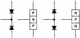
Fig. 1 -Transistor diode junction equivalent schematic.
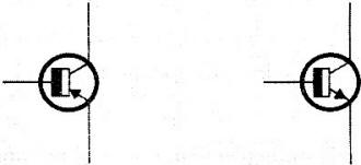
Fig. 2 - NPN and PNP transistor schematic symbols.
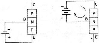
Fig. 3 - Base-emitter and collector-emitter biasing.
Transistors have puzzled technicians for nearly a decade and there appears to be no
sign of easing the strain. Each year more transistorized equipment is introduced in both
television and hi-fi equipment. To keep up to date we must learn efficient transistor
servicing procedures.
Many articles have been devoted to transistor troubleshooting and all of them have
leaned heavily on theory. But many successful technicians working on vacuum-tube circuits
do not have a solid foundation in vacuum-tube theory, so perhaps the solid-state troubleshooter
does not necessarily need theory. Let's look at transistors from a troubleshooter's standpoint
and minimize the theory.
For those of you with experience with tubes here is a comparison of transistors and
tubes: A transistor is somewhat like a tube: Corresponding elements are:
- Tube-Transistor
- Cathode-Emitter
- Grid-Base
- Plate-Collector
There are two important differences:
- The tube is a voltage amplifier.
- The transistor is a current amplifier.
The grid of a tube usually has an opposite potential to the cathode and plate of a
tube, but the transistor base potential is between the emitter and collector potentials.
Just Two Diodes
Transistors are further complicated as there are two types which operate with opposite
bias and supply voltage polarities.
Yet it is easy to determine proper polarities for bias and supply voltages and what
voltages we can expect in standard circuit configurations for each type.
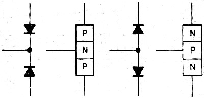
The two basic types are, of course, pnp and npn. Physical and electrical characteristics
of pnp and npn transistors are shown in Fig. 1. Both transistors are shown electrically
as two diodes wired back to back. In the pnp type the cathodes are tied together; in
the npn type the anodes are connected. The junction represents the base connection with
the emitter or collector at either end.
Two common symbols for both pnp and npn transistors are in Fig. 2. Note that the arrows
in both the diodes and the transistor symbol point in the same direction. Remember this
and you cannot go wrong.
Normal Circuit Parameters
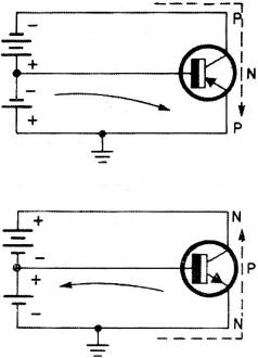
Fig. 4 - Base current direction for PNP and NPN transistor.
In conventional circuits a small forward bias, normally 0.2 to 0.7 volt, is applied
to the emitter junction. An easy way to remember which polarity is required to forward-bias
a junction is to note that, when a negative voltage is applied to an n-element and a
positive voltage to a p-element of a pn junction, it is forward-biased. This is shown
in Fig. 3. The letters tell you the crystal type in each element. That is, pnp stands
for p-type (crystal) emitter, n-type base and p-type collector. npn stands for n-type
emitter, p-type base and n-type collector.
In other words, for a forward-biased emitter junction, a pnp transistor requires a
negative voltage on the base with respect to the emitter. To forward-bias an npn transistor
emitter junction a positive voltage on the base, with respect to the emitter, is required.
The collector circuit, on the other hand, requires a back-bias or reverse bias. So
in a pnp transistor, a negative voltage is required on the collector with respect to
the base and the opposite for an npn transistor. Circuits with these typical configurations
are shown in Fig. 4. Note that the bias batteries are connected so they aid one another.
The Need for Biasing
Biasing is used in transistor circuits for the same reason that it is used in tube
circuits-to set up a static operating point. Without proper bias, what was intended to
be a class-A amplifier might operate class-B.
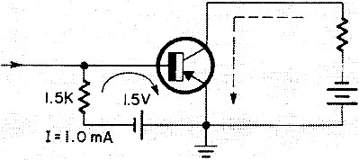
The simplest bias is accomplished with a single-resistor network. A common-emitter
amplifier with a single bias resistor is shown in Fig. 5. Since the emitter-junction
resistance is quite low, the base bias current can be calculated by dividing the bias
voltage by base bias resistor. The base resistance is ignored because it is very small
compared to the base bias resistor.
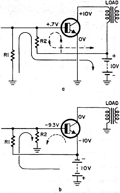
In Fig. 6-a, the negative terminal of the power supply is grounded. In Fig. 6-b, the
positive terminal of the power supply is grounded. Each circuit's operation is identical.
The resistors form a voltage divider network and selection of various values can result
in any voltage between the supply and zero volts to appear at the base of the transistor.
If there is a 0.7-volt difference between base and emitter, the transistor is turned
on and emitter/collector current flows. If this voltage difference is reduced, less collector/emitter
current flows. Conversely if this voltage difference is increased, collector/emitter
current increases.
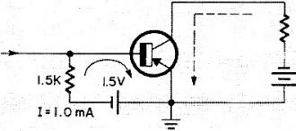
Fig. 5 - PNP transistor DC biasing.
In Fig. 6-a, if a 10-volt supply is used, R2 will be approximately 9 times as large
as R1 and +0.7-volt appears at the base. In Fig. 6-b, the values of R1 and R2 stay the
same, but their relative positions are reversed to effect a +9.3-volt potential on the
base. Either way, the base is +0.7-volt with respect to the emitter. The voltages shown
are typical for a silicon transistor. Note that the base voltage is closest to the emitter
voltage and between collector-emitter voltage.
An important consideration is the polarity and magnitude of voltage that must be applied
to the base/emitter junction to turn the transistor "on" and cause electron flow between
emitter and collector. While a tube requires bias voltage to reduce electron flow, the
transistor requires bias current to cause electrons to flow. A tube with zero bias between
grid and cathode generally has heavy current flow while a transistor with zero bias between
base and emitter is shut off and no current flows between collector and emitter.
To forward-bias or "turn on" a transistor, a small voltage is applied between the
base and emitter elements. When measured from the emitter, the polarity of this bias
voltage is the same as the collector voltage but its value is much lower.

Fig. 6 - Emitter self-biasing.
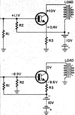
Fig. 7 - Emitter stabilizing resistor.
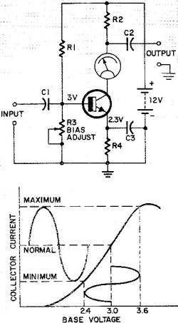
Fig. 8 - Class A (linear) transistor biasing.
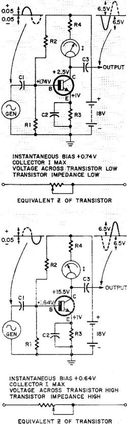
Fig. 9 - Input - output voltage waveforms.
Remember, as the voltage on the base element changes in the direction of the collector
potential, the emitter/collector current increases. If the voltage on the base element
moves in the direction of the emitter potential, the emitter/collector current decreases.
This is true regardless of whether the transistor is silicon or germanium and npn or
pnp.
In Fig. 7, resistor R3 is in series with the emitter. It stabilizes collector current
and is referred to as a stabilizing resistor. As collector current flows through emitter
resistor R3, a voltage is developed which opposes the forward-bias voltage. The effect
of R3 is to oppose any change in current flow since the voltage across it is in series
with the forward-bias voltage. For example, if collector current increases, the voltage
drop across R3 increases and reduces the effective forward bias which, in turn, reduces
collector current.
Conversely, if collector current decreases, less voltage is developed across R3 and
the effective forward bias increases. This, in turn, increases collector current. Adding
an emitter resistor stabilizes a transistor with respect to collector-current variations
which occur for a variety of reasons. The most common cause is an increase in collector
current as a result of temperature increase.
When troubleshooting, the voltage drop across the emitter resistor is an important
test point for checking circuit operation. A higher than normal emitter voltage generally
indicates excessive collector current. This can be caused by a shorted transistor or
a bias defect. A lower than normal emitter resistor voltage would indicate an open transistor
or bias defect.
Class-A Amplifier
A transistor stage set up for class-A or linear operation is shown in Fig. 8. In this
stage. bias resistor R3 is shown as an adjustable unit, so some desired collector current
will flow. This control can be used to show how the transistor amplifies the input signal.
The base voltage-collector current curve in Fig. 8 shows the collector current for
several bias voltages. The horizontal line shows bias voltages developed across bias
resistor R3. The vertical line shows values of collector current for each value of bias
and we will neglect the effect of emitter resistor R4.
Note the mark on the bottom line indicating 2.4 V. This actually means 0.1 V between
the base and emitter since the emitter is at +2.3 V. This mark corresponds with a line
on the vertical column marked "minimum" as indicated by the dotted lines. This means
that, with 0.1 V forward bias, only a small amount of collector current will flow.
If R3 is adjusted to make the base voltage become 3 V (0.7 V between base and emitter),
the collector current increases. Referring again to the curve, we see that the collector
current has increased to the mark on the vertical column marked "normal".
If R3 is adjusted to make the base voltage become +3.6 V (1.3 between base and emitter).
there will be an increase in collector current. The collector current has increased to
the "maximum" level.
From this we can see that by varying the base voltage, we can produce any desired
value of collector current. In practice, the emitter voltage would not remain constant
with different values of collector current. This action is similar to cathode-voltage
variation in a tube.
An AC signal fed to the base element can also cause collector-current changes. Referring
again to Fig. 8, we adjust R3 to make the base voltage become +3 V. This causes a collector
current that corresponds to "normal" on the curve. The collector current through R2 causes
a voltage drop so about half the supply voltage appears at the collector. These are the
necessary conditions for a linear stage (amplification without distortion).
An AC generator supplies a signal between the base of the transistor and chassis ground
in Fig. 9. This signal at any instant will add or subtract from the de bias supplied
by bias resistors R1 and R2. Capacitor C2 provides an AC bypass across R3 at the signal
frequency.
In Fig. 9-a the generator is passing through its maximum positive excursion and is
producing a peak +0.05 V. This voltage will add to the +1.69 V DC bias voltage and cause
a total instantaneous voltage between base and ground of +1.74 V. From the curve in Fig.
8, we see that this corresponds to maximum current through the transistor. This is indicated
by the current meter connected in series with the collector of the transistor.
The increased current through R4 causes a larger voltage drop, so that for an instant
the collector voltage drops to approximately 2.5.
The result of the negative half-cycle of the generator is shown in Fig. 9-b. This
negative 0.05-V excursion subtracts from the 1.69-V bias, so that for an instant the
voltage between base and ground is 1.64 V. The curve in Fig. 8 shows that this corresponds
to minimum collector current. The reduced current causes a smaller voltage drop across
R4 and allows the collector voltage to rise to approximately +15.5.
From this we can see that an input signal of 0.1 V peak-to-peak can cause a collector
or output signal of 13 V peak-to-peak. Also, phase inversion occurs. The DC and AC voltage
excursions shown demonstrate amplification of the transistor. Capacitor C2 is large enough
to bypass R3, so that no AC signal is lost across this resistor. The voltage at the emitter
will reflect any average current change through the transistor. Emitter voltage is a
good indicator of transistor conduction. If this voltage is too high, the transistor
current is too high. If it is low, the current is too low.
Diode Stabilization
Some amplifiers require a different type of bias stabilization since their primary
purpose is to increase power. The circuits discussed are designed to maintain constant
current. This would defeat the purpose of the push-pull amplifier, so another method
is used.
The most common stabilization method used for these amplifiers is to use bias elements
which are temperature-sensitive. One method, shown in Fig. 10, is to use a diode made
from the same material as the transistor.
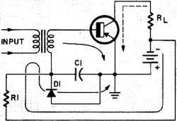
Fig. 10 - Diode stabilization.
The diode is fed with a constant current through R1. The voltage drop across the diode
biases the transistor and is inversely proportional to its temperature. In other words,
as the temperature of the transistor and diode increases, the resistance of the diode
decreases and the voltage drop across the diode decreases lowering the bias voltage the
necessary amount.
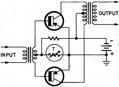
Push-Pull Stabilization
Thermistors are frequently used to stabilize push-pull output stages. Thermistors
have a negative temperature coefficient of resistance. A circuit using a thermistor for
bias stabilization is shown in Fig. 11. The current through the thermistor is held relatively
constant by the high series resistance. The voltage drop across the thermistor supplies
the actual transistor bias. Since the compensation in this circuit is often greater than
desired a parallel resistor is sometimes added to the circuit to decrease its sensitivity.
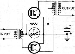
Fig. 11 - Push-pull amplifier configuration.
Note that the purpose of the temperature sensing element is, not to compensate for
ambient temperature, but to compensate for the junction temperature of the transistor.
Consequently, whether the sensing element is a diode or a thermistor it should be located
intimately with the transistor or transistors that it controls.
Posted December 6, 2018
|