Wax nostalgic about and learn from the history of early
electronics. See articles from Radio & Television News, published 1919-1959. All copyrights hereby
acknowledged.
In April of 1952 when this article
appeared in Radio & Television News magazine, the bipolar junction transistor
(BJT) had only made it out of the experimental laboratory of Messrs. Bardeen, Shockley,
and Brattain at Bell Labs a mere three years earlier in December of 1948. It did
not take long for commercial production to begin. Along with being a great primer
for anyone new to transistors, herein is also some background on how the now ubiquitous
BJT schematic symbol was created. Interestingly, only Dr. William Shockley is mentioned,
making me wonder whether the contributions of Dr. John Bardeen, and Dr. Walter
H. Brattain was not widely publicized early on. Not to worry, though, because all
three were duly recognized as recipients of the 1956 Nobel Prize in Physics. See this month's editorial called
"The Amazing Transistor."
The Junction Transistor
Comparative size of the new junction transistor and a standard
miniature type 6AK5, which is 3/4" in diameter.
By H. S. Renne
Technical Editor Radio & Television News
Details on Bell Laboratories' newly-developed unit and a discussion of some potential
uses.
There was a tremendous amount of excitement among electronic engineers when the
first point-contact transistor was announced by Bell Telephone Laboratories some
four years ago. This initial enthusiasm, however, was soon replaced by a great deal
of hard work at the laboratories where efforts were made to iron out the "bugs"
existing in the original design, and to ready the device for mass production. These
goals have now been reached and reliable, uniform point-contact transistors are
in limited production.
The original interest in transistors was given a new stimulus last July with
the announcement of the junction transistor. Based on theoretical work at Bell Laboratories
by Dr. William Shockley, this new device possessed qualities which seemed to indicate
that in many respects it would prove to be superior to the point-contact type of
transistor. Intensive research and development work is now in progress all over
the country to determine its limitations and capabilities and to prepare it for
mass production.
Transistors are constructed of a metal called germanium, which is classed as
a semiconductor. Conduction of electricity through germanium can take place either
by a .flow of electrons or by a flow of so-called "holes" which are, in effect,
an absence of electrons. The result is similar to what would occur if an electron
were replaced by a positive charge. The type of conduction is determined by very
slight amounts of impurities in the germanium. If these impurities are such that
conduction takes place by means of electrons, the germanium is of the "N" type.
If conduction is by means of "holes," the germanium is known as the "P" type.
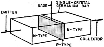
The basic construction of the junction transistor is shown in Fig. 1. It
consists essentially of a very thin wafer of "P" type germanium cut from a single
crystal and placed between two tiny bars of "N" type germanium, also cut from a
single crystal. Because of this construction, the junction transistor is often
referred to as the "NPN" transistor.
Fig. 1 - Basic construction of the junction transistor.
Two types of germanium are used.
This new device has many characteristics which entitle it to be called the first
serious rival to the vacuum tube. Its amplifying properties are in many respects
superior to conventional tubes, and it is far more rugged with respect to shock
and vibration than any known tube. It is much smaller (about half the size of a
pea), and has an expected service life greatly exceeding that conventional tubes.
Fig. 3 shows the form of presentation which has been adopted for the junction
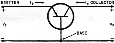
transistor. The base is the center or "P" type section of germanium; the collector
and emitter are the "N" type sections.
Power amplifications as high as 51 db (100,000 times) have been achieve! with
specific units, and it is reasonable to assume that this figure can be approached
or even exceeded in production units. The actual power output rating of the transistor
itself is rather small, depending primarily on the cross-sectional area of the germanium
at the junction. Most of the experimental units use a germanium rod about a sixty-fourth
of an inch in diameter, and have an output rating on the order of 50 milliwatts,
heat dissipation within the unit being the limiting factor. One transistor has been
assembled with a cross-sectional area of a square centimeter which has a rating
of two watts, and still higher-powered units are possible.
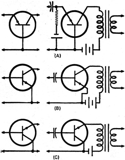
A variety of input and output impedances may be achieved by connecting the transistor
in different ways. Fig. 2 shows the three possible connections, together with
a corresponding practical circuit for each.
Fig. 2 - How the input and output impedances may be varied
by connecting the junction transistor different ways. In each case. the connection
is shown along with a corresponding practical circuit. (A) Grounded-base circuit.
(B) Grounded-emitter circuit. (C) Grounded-collector hookup. See article for a complete
description of their possible applications.
The arrangement in Fig. 2A is called the grounded-base circuit, characterized
by a low input impedance and a high output impedance. Typical values would be from
about 50 to 250 ohms for the former, and from 1.5 to 13.5 megohms for the latter.
These values depend to quite a large extent on the construction of the transistor,
as well as the amount and kinds of impurities present in the germanium. Power gains
of 40 to 50 db can readily be achieved with this arrangement when impedances are
matched, and appreciable gains can be obtained with a load resistance of only a
few thousand ohms. One advantage of the latter arrangement is that the gain is almost
completely independent of those transistor properties which vary from unit to unit.
When amplifier stages of this type are cascaded, a matching transformer should be
used.
The second type of connection, illustrated in Fig. 2B, is known as the grounded-emitter
circuit. This is the most desirable circuit for many applications. Input impedance
is higher and output impedance much lower than for the grounded-base arrangement,
typical values being 250 to 1500 ohms for the input impedance, and 250,000 ohms
to 1.5 megohms for the output impedance. Maximum available gain is over 50 db. In
the practical circuit of Fig. 2B, the base will float at a certain potential.
If a different potential is desired, various arrangements for biasing may be used.
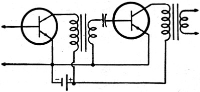
A two-stage amplifier utilizing this circuit and having a power gain of about 90
db is shown in Fig. 4. This amplifier is pictured at the right of Fig. 5.
The power gain available from the grounded-collector stage, shown in Fig. 2C,
is rather low, about 15 to 20 db, but the circuit has certain other advantages which
make it desirable. Input impedance is high although varying widely with the load
resistance. Output impedance likewise depends upon input loading, but in general
is quite low. Thus, this circuit arrangement takes on the characteristics of a cathode
follower, and if the source impedance is on the order of a few thousand ohms, the
output impedance may be 25 ohms or less. Audio enthusiasts would undoubtedly like
to use this device to drive a voice coil direct, without using an output transformer!
The junction transistor is especially suited for use at very low power levels.
Its efficiency is exceptionally high, closely approaching the theoretical maximum
of 50% for Class A and 100% for Class C amplification. Thus, the input battery power
required can be extremely small. For example, an audio oscillator (shown at left,
Fig. 5) has been built which operates satisfactorily with an input power of
only 0.08 microwatt, consisting of 50 millivolts at 1.5 microamperes! To demonstrate
the small power required, Mr. R. L. Wallace, of Bell Laboratories, powered this
oscillator with the output of a photovoltaic cell exposed to room illumination.
In another experiment, he formed a battery by wrapping a dime in a piece of paper
which he had previously moistened by chewing on it. The moist paper became one electrode
of the battery, and the dime the other. In both cases, the output was sufficient
to be audible from an ordinary head-phone.
Fig. 3 - Symbol which has been adopted to designate the
junction transistor.
Fig. 4 - A grounded-emitter type circuit used as a two-stage
amplifier which has a power gain of approximately 90 db.
Fig. 5 - (Left) Audio oscillator which operates with an
input power of 0.08 micro watt and (Right) a two-stage audio amplifier which was
built using the circuit of Fig. 4.
Mr. Wallace also performed some interesting calculations to show that this device
could really be called a "flea-power" device. Assuming a dog flea weighing one milligram
and jumping to a height of 50 centimeters, both of which are reasonable figures,
he calculated that the flea, in making one such jump every minute, would use approximately
the same amount of energy as the minimum required to keep the oscillator functioning!
It is logical to assume, therefore, that satisfactory amplifiers can be built which
would operate on comparably small amounts of input power.
It should not be supposed from the previous discussion that this transistor is
a cure-all for everything. There are disadvantages which mayor may not be overcome
in future development work. One is the problem of frequency response. Maximum gain
of the junction transistor is attained at frequencies on the order of a few kilocycles,
with the gain falling off rapidly as the frequency increases. (Usable gains up to
one megacycle and more have been realized, however.) One factor affecting frequency
response is the transit time of the electrons and "holes" through the "P" layer.
Making this layer thinner should increase the frequency response, but it would also
increase the capacity between the two "N" electrodes. A thickness of about a thousandth
of an inch has been used for this "P" layer.
Another problem is that of the mass production of these items. The amount of
impurities in the germanium must be controlled very carefully, as variations of
as little as one part in one hundred million can change the properties of the transistor.
Also, there is the mechanical problem of fastening leads to such small pieces of
germanium. How this is done on present samples has not been revealed. The units
must be made to have uniform characteristics in production, so that a transistor
in a piece of equipment may be replaced by another transistor without re-engineering
the whole circuit. Samples which have been tested have been found to be very temperature-sensitive,
although operation is completely satisfactory over normal temperature ranges.
These problems are gradually being overcome and it is expected that production
samples on a limited basis will be available not too many months hence.
Here is a device which most certainly will give the vacuum tube a run for its
money - if not completely replace it - in the majority of applications. It has practically
no heat loss, making. it useful in applications where very large numbers are required,
such as electronic computers of various kinds. It is extremely rugged, reliable,
and has an almost indefinite life. A typical value of transconductance is 33,000
micromhos per milliampere, and of amplification factor, 39,000. Since the output
impedance of a cathode follower is 1/Gm, an output impedance of 5 ohms
is possible with a current of 5 ma. The Gm is inversely proportional
to the absolute temperature, so that fantastically large values can be achieved
by supercooling. Its noise figure is better than some vacuum tubes, being as low
as 10 db and less on some of the units which have been tested.
These characteristics are certainly sufficient to justify the excitement and
anticipation brought about by the announcement that such a device had been developed.
Lest anyone be misled, it would be well to emphasize that this device is not commercially
available at the present time, but commercial production is definitely planned for
the near future.
Newsreel from 1956, showing William Shockley, Walter Brattain
and John Bardeen receiving the Nobel Prize for the transistor.
Posted April 22, 2022 (updated from original post on 1/5/2016)
RF Cafe began life in 1996 as "RF Tools" in an AOL screen name web space totaling
2 MB. Its primary purpose was to provide me with ready access to commonly needed
formulas and reference material while performing my work as an RF system and circuit
design engineer. The World Wide Web (Internet) was largely an unknown entity at
the time and bandwidth was a scarce commodity. Dial-up modems blazed along at 14.4 kbps
while tying up your telephone line, and a nice lady's voice announced "You've Got
Mail" when a new message arrived...
Copyright 1996 - 2026
All trademarks, copyrights, patents, and other rights of ownership to images
and text used on the RF Cafe website are hereby acknowledged.
All trademarks, copyrights, patents, and other rights of ownership to images
and text used on the RF Cafe website are hereby acknowledged.