

RF Cascade Workbook for Excel
RF & Electronics Symbols for Visio
RF & Electronics Symbols for Office
RF & Electronics Stencils for Visio
RF Workbench
T-Shirts, Mugs, Cups, Ball Caps, Mouse Pads
Espresso Engineering Workbook™
Smith Chart™ for Excel
|
 |
Analog Devices’ Dual Adaptive Clock Translator Supports Wide Range of Wired Network Applications
Including OTN De-Mapping and High-density Line Cards
|
July 27, 2012 Press Release

NORWOOD, Mass.--(BUSINESS WIRE)--
Analog Devices, Inc. (ADI) today introduced a
fully-programmable, jitter-attenuating, dual-clock translator IC (integrated circuit) to address the timing
requirements of high-speed optical transport network (OTN) applications and high-density line cards. The
AD9559 quad-input multiservice line card adaptive clock
translator simultaneously supports different standard frequencies for wired communications applications, including
synchronous Ethernet, SONET/SDH, 1/10/100G Ethernet, Fiber Channel, and other applications that require low
jitter, flexibility and fast time-to-market. The AD9559 translator IC synchronously converts any standard input
frequency to any standard output frequency at up to 1.25 GHz with sub-400-fs RMS (root mean square) total jitter
over a 12-kHz to 20-MHz integration bandwidth. The AD9559 replaces two synchronous timing devices with a single
IC, helping designers with board space constraints and cost optimization.
 Download
data sheets and order samples: http://www.analog.com/AD9559 Download
data sheets and order samples: http://www.analog.com/AD9559
For the single-channel version of this device, visit
http://www.analog.com/AD9557
The AD9559 is the
industry’s most flexible high-performance dual adaptive clock translation solution for high-density line cards and
OTN applications. Adaptive clocking allows the DPLL (digital PLL) divider ratios to be changed while the DPLL is
locked. This enables the frequency at the output to be dynamically adjusted over a ± 100 ppm range, around the
nominal output frequency, with a resolution in frequency step as low as sub-0.1 ppb, without breaking the loop and
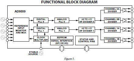
reprogramming the part. The AD9559 IC’s parallel DPLL architecture allows the user to generate output clocks that
are completely independent of each other. Each of the two DPLLs can be synchronized to one of up to four input
references, and each DPLL generates two output clocks. The DPLL allows for reduction of input time jitter or phase
noise associated with the external references.
The AD9559 continuously generates a clean (low jitter)
valid output clock, even when all references have failed, by means of a digitally-controlled loop and holdover
circuitry. The built-in programmability of the AD9559 clock translator allows network line card designers to use
the same component in many different board designs, limiting the number of components needed and reducing overall
system cost.
At 10 mm x 10 mm in size, the AD9559 clock translator provides a compact, frequency agile,
cost effective clock for line card designers. Applications include data communications, next-generation wired
networking applications, test and measurement, high-speed data acquisition, video applications, and wireless base
station controllers.
Key Features of the AD9559 Quad-input Dual Adaptive Clock Translator
- Dual DPLL architecture, with four reference inputs (single-ended or differential) going to an input
crosspoint
- Supports adaptive clocking and gapped clock input reference for OTN de-mapping applications
- Supports GR-1244 Stratum 3 stability in holdover mode
- Smooth reference switchover with virtually no disturbance on output phase.
- Supports Telcordia GR-253 jitter generation, transfer, and tolerance for SONET/SDH up to OC-192 Systems
- upports ITU-T G.8262 Synchronous Ethernet slave clocks
- Supports ITU-T G.823, G.824, G.825, and G.8261
Availability, Pricing and Complementary Parts
Product Availability Operating
Temp Range Price each in 1,000 quantity Packaging
AD9559 Full Production -40˚C to 85˚C $19.26 10-mm
x10-mm 72-lead LFCSP
Complementary components include ADI’s ADCLK9XX series of clock fanout buffers,
including the
ADCLK944, which achieves jitter performance of 25 fs (typical) over the integration bandwidth of 12 kHz to 20
MHz. For power management, the ADP150 or ADP222 ultralow noise, low dropout, linear regulators, or the ADP1829
dual PWM switching buck controller are recommended. For additional support, connect with engineers and ADI product
experts on EngineerZone™, an online technical support community:
http://ez.analog.com/community/clock_and_timing
About Analog Devices
Innovation, performance, and excellence are the cultural
pillars on which Analog Devices has built one of the longest standing, highest growth companies within the
technology sector. Acknowledged industry-wide as the world leader in data conversion and signal conditioning
technology, Analog Devices serves over 60,000 customers, representing virtually all types of electronic equipment.
Analog Devices is headquartered in Norwood, Massachusetts, with design and manufacturing facilities throughout the
world. Analog Devices is included in the S&P 500 Index.
This release may be deemed
to contain forward-looking statements intended to qualify for the safe harbor from liability established by the
Private Securities Litigation Reform Act of 1995. These forward-looking statements include, among other things,
our statements regarding expected benefits of our acquisition of Multigig and expected advances in our technology
and product development efforts, that are based on our current expectations, beliefs, assumptions, estimates,
forecasts, and projections about the industry and markets in which Analog Devices operates. The statements
contained in this release are not guarantees of future performance, are inherently uncertain, involve certain
risks, uncertainties, and assumptions that are difficult to predict. Therefore, actual outcomes and results may
differ materially from what is expressed in such forward-looking statements, and such statements should not be
relied upon as representing Analog Devices’ expectations or beliefs as of any date subsequent to the date of this
press release. Important factors that could cause actual results to differ materially from the results described,
implied or projected in any forward-looking statements include: sovereign debt issues globally, any faltering in
global economic conditions and financial markets, erosion of consumer confidence and declines in customer
spending, unavailability of raw materials, services, supplies or manufacturing capacity, changes in geographic,
product or customer mix, adverse results in litigation matters, and other risk factors described in our most
recent filings with the Securities and Exchange Commission. We do not undertake any obligation to update
forward-looking statements made by us.
Follow ADI on Twitter at
http://www.twitter.com/ADI_News.
Subscribe
to Analog Dialogue, ADI’s monthly technical journal, at:
http://www.analog.com/library/analogDialogue/subscribe.html
Contacts
Jim Surber
Analog Devices
336-605-4365
jim.surber@analog.com
Date Posted 7/27/2012
|
 |
|

 |


 Download
data sheets and order samples: