|
November 15, 1965 Electronics
 [Table of Contents] [Table of Contents]
Wax nostalgic about and learn from the history of early electronics.
See articles from Electronics,
published 1930 - 1988. All copyrights hereby acknowledged.
|
I remember in one of my circuits
classes in college when the gyrator was introduced, and I thought it was an ingenious invention.
The gyrator circuit, implemented with an operational amplifier (opamp) and a couple
resistors and capacitors, changed its measured impedance type from that of a capacitance
to that of an inductance. That is, its impedance represents an
R + jX Ω format. Frequency
limits are imposed by a combination of the self-resonant frequencies of the resistors
and capacitors as well as the
gain-bandwidth
product (GBWP) of the opamp, and power handling is primarily limited by the
opamp's voltage and current capabilities. You might ask why, with all those constraints
on its use you would even want to use a gyrator circuit? The answer is that within
its limitations, the gyrator often represents a less expensive and more compact
version of a physical inductor. This is particularly true with integrated circuits
(ICs) where, unless it is a
monolithic microwave IC (MMIC) operating in the tens of gigahertz
region, there is no space available on the die for a printed metallic inductor with
enough inductance to be useful. Any inductors would need to be mounted off-chip
on the PCB with I/O pins interfacing to the IC. Gyrators onboard ICs have made filtering
functions available into the tens of megahertz realm nowadays with the extremely
high GBWP of modern opamps.
Six Possible Routes to Noninductive Tuned Circuitry
 Inductance is nearly impossible to put into
an IC, but the effect can be achieved using RC networks, digital filtering, acoustic
resonators or semiconductor delay lines. Inductance is nearly impossible to put into
an IC, but the effect can be achieved using RC networks, digital filtering, acoustic
resonators or semiconductor delay lines.
By Vasil Uzunoglu, Applied Physics Laboratory
Johns Hopkins University, Silver Spring, Maryland
When circuit designers began shifting from tubes to transistors, they also began
to seek ways to do away with bulky transformers and coils. One approach was to use
resistance-capacitance (RC) networks as substitutes for low-frequency inductance-capacitance
(LC) circuits.
With the arrival of integrated circuits, the designers no longer have a choice.
No practical method has been found for putting usable amounts of inductance into
an integrated circuit, despite some qualified successes. Multilayer thin films,
deposited on monolithic chips, can provide a few microhenries of inductance; however,
such small inductances are not adequate for operation at frequencies lower than
a few megacycles per second. More recently, an electromechanically resonant field-effect
transistor has been introduced [Electronics, Sept. 20, 1965, p. 84], but its ultimate
utility is yet to be proved.

Two typical notch-filter RC circuits are the parallel-T at left
and the bridged-T, center. The attenuation vs. frequency relationships for minimum
and nonminimum phase-shift networks are similar, as shown at right.
The engineer who wants to design a frequency-sensitive integrated circuit must
find some way to duplicate the effect of inductance. There is no single perfect
substitute for inductance, but at least six techniques are known; the choice depends
on the requirements of the system being designed.
Three of these techniques employ resistor-capacitor networks. One uses RC notch
filters in the feedback path; another, RC circuits in the forward transmission path;
and the third, negative impedance converters. These methods have the same disadvantage:
in some applications, particularly those in which high Q values (100 or larger)
are needed, RC networks have a tendency toward instability. In such cases, three
other techniques are possible: sampling (digital filtering), using acoustic resonators,
and using semiconductor delay lines.
The choice of one of these six approaches depends on the specific requirement;
it should be based on a careful evaluation of the specifications, and on the comparison
of these requirements with the inherent advantages and disadvantages of each method.
Notch-Filter Feedback
A notch-filter circuit is one whose gain-versus-frequency characteristic exhibits
a steep drop or rise at resonance. A typical voltage-gain curve for a notch-filter
circuit is shown on page 115. Also shown are two examples of notch-filter circuits:
the parallel-T network and the bridged-T network.
Notch-filter circuits fall into two general categories: one called a minimum
phase-shift type, the other called a nonminimum type. The minimum type exhibits
a phase shift less than ±90°. The latter can produce shifts in phase
from 0 to 360°. This is shown by the curves on page 115. Minimum-phase-shift
circuits are usually fabricated with lumped elements, nonminimum types are made
with either lumped or distributed elements.

Phase characteristics for minimum and nonminimum phase-shift
notch filters differ greatly, although attenuation characteristics are similar.
The nonminimum circuit produces phase shifts from 0° to 360°; the minimum
filter circuit exhibits shifts smaller than ±90°.

Simplified representation of an amplifier with a notch filter
in the feedback path. The filter may be of either the minimum or nonminimum phase-shift
type.
When high Q is desired, the nonminimum type is preferable, but such circuits
can be unstable. For a high degree of stability, when lower Q can be tolerated,
the minimum type is usually best. For stable oscillator circuitry,2 however,
the nonminimum circuit is preferred because of the sharper phase shift with changes
in frequency.
Either type of network can be constructed using a bridged-T arrangement. If a
minimum phase-shift circuit is desired, lumped resistors are used for R1
and R2. For nonminimum phase shift, R1 and R2 should
be distributed elements. Both minimum and nonminimum phase-shift networks can be
realized with lumped elements using the parallel-T circuit but the nonminimum network
requires more reactive (capacitive) components.
A nonminimum phase-shift circuit must have at least three capacitors.1
However, the circuit can be designed so that the distributed resistors also contribute
the required capacitance values.
A simple block diagram for an amplifier that incorporates a notch filter in the
feedback path is shown on this page. Regardless of whether it is a minimum or nonminimum
circuit, a notch filter must satisfy two circuit requirements: the required Q must
be obtained, and the insensitivity to minor variations in operating conditions must
be sufficient to prevent oscillations.
The closed-loop transfer function (gain including feedback) is given by:

where AT is the total closed-loop gain, eout
is the closed-loop output voltage, ein is the
input voltage, A(s) is the open-loop gain of the amplifier
(gain without feedback), β(s) is the feedback factor,
β(s) = Δeout/eout, where
Δeout is the feedback voltage.
To achieve the required Q without oscillations, the amplifier design must satisfy
the conditions that |A(s)β(s)| ≈ 1 and the
phase shift over the loop is approximately 360°. If the |Aβ| is actually unity,
and the phase shift 360°, oscillation would occur. Therefore, this product and
phase angle should be approached but not actually reached.
The sensitivity of the gain for a closed-loop system1 may be defined
as:

where dAT is the variation caused by
dA(s)
etc., where T is the period of the modulating function. The multiplied signal
is then fed to a low-pass filter, h(t). The frequency
difference between f(t) and ein
must lie within the bandpass limits of h(t). The outputs
from the filters are multiplied again by functions Φ(t), Φ(t
- T/N, Φ(t - 2T/N), in synchronism with f(t).The
outputs from all branches are added up; this sum constitutes the final output. The
entire operation simulates the functioning of a series-tuned LC network that passes
a desired frequency and rejects all other frequencies.

Pole plot for bandpass filter.
Because the modulating signals are sinusoidal, the driving-point (input) impedance
of the entire network can be represented by.

where ωo is 2π
times the center frequency and K is a constant determined
by the circuit elements. Equation 7 is also the expression for the impedance of
an inductor in series with a capacitor.
If the modulating time function, f(t) is an impulse
and if the input signal is supplied by a current source each modulator can be replaced
by a simple switch. Then the input and output modulating signals are equivalent
to a pair of rotary switches with N contacts as a common shaft that rotates at
1/T = ωo/2 cycles per second. Each low-pass
filter, h(t), must have a bandwidth much lower than
fo, the center frequency desired for the entire
bandpass-filter network.
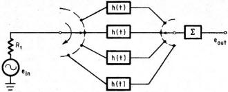
When only one passband is desired, the bandpass-filter circuit must have at least
three h(t) sections to get rid of the harmonics (multiples
of ωo). A mechanical sampling section for eliminating
harmonics8 is depicted at the left. Each filter samples at a different
time. As the switch's operating speed increases, the effectiveness of stopping the
harmonics improves.
The extent of time during which the brushes remain on each contract is given
by:
t1 = T/R1
and t2 = T/R2 (8)
where t1, t2
are contact times, R1 is the source impedance,
and R2 is the load impedance.
An advantage of this technique is that the filter can be tuned at different frequencies
without altering the system. The center frequency of the filter can be changed simply
by changing the frequency of the timing source that controls the switching rate.
With this method, it is possible to achieve Q's of 5,000 to 10,000 at a few hundred
kilocycles per second. These values are much higher than those that can be obtained
with any type of stable filter using RC networks.
Comb Filters

Mechanical switching circuit for frequency filtering. Each filter
represented by h(t) samples at a different time. The rejection of harmonics is improved
by increasing the switching speed.

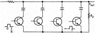
Electrical equivalent of the comb data-sampling circuit.
Besides its use as a very narrow bandpass filter, the same system can be used
to build comb filters,8 with bandpass centered at multiples of
ωo. In the simplified mechanical analog
of a comb system, shown on page 119, t1 is
the time required by the brush to move from one contact to another. The input signal
is applied through a high-value resistor to brush A (upper arrow on diagram). While
A is in contact with the corresponding capacitor, the capacitor begins to charge,
so that its potential approaches that of the input signal. However, the time constant
of the RC network is much higher than the dwell time of the brush on one segment,
so that it takes a certain time for the capacitor to charge; before the capacitor
can build up an appreciable charge, the brush changes position.
If the signal frequency is a multiple of the frequency of rotation, the signal
will have the same value each time the brush comes in contact with a given segment.
Thus, after a certain number of revolutions, the potential across each capacitor
will attain its maximum value; this means that the locus of charge on the capacitors
is an indication of the input-signal level. However, this system prevents the buildup
of random signals and signals that are periodic, or of signals that are periodic
but whose frequency is not a multiplier of the rotational frequency. This suggests
that such a sampling filter may be used in detecting weak periodic signals in the
presence of noise.
An electrical circuit equivalent of the mechanical data-sampling filter just
discussed is shown on this page. This circuit was introduced by G. H. Danielson."
Acoustic Resonators
The acoustic-resonator technique requires mounting piezoelectric crystal onto
a monolithic silicon chip. The installation is difficult, because the crystal must
be positioned so that it is allowed to vibrate freely.
When an electric wave is applied to the resonator, traveling acoustic waves are
generated at the resonant frequency.2 These traveling waves are reflected
when they reach a boundary. If the resonator is well designed, the initial transmitted
and reflected acoustic energy are added together, causing an intense standing wave.
This acoustic wave is converted back to an electric wave at the point of application.
At this point the electrical circuit sees the equivalent of a parallel circuit tuned
to the resonant frequency. To achieve high Q, the losses must be minimized. The
acoustic wave, as it bounces back and forth, is subject to high losses. The use
of an acoustic resonator in microelectronic blocks is feasible if the supporting
medium of either the resonator or substrate does not absorb the mechanical vibrations
or permit leakage of the acoustic energy. Therefore, solid mounting of a conventional
piezoelectric resonator is not possible. Piezoelectric materials such as cadmium
sulfide and zinc oxide have been used for acoustic resonators.
Semiconductor Delay Lines
Semiconductors delay lines1 are relatively easy to integrate because
only one diffusion is required in their manufacture. Only resistive elements used;
capacitors are eliminated. In the semiconductor delay line shown on this page, the
distance between the two n regions determines the delay time and, therefore, the
frequency.
Minority carriers are injected at the junction on the left and, being subject
to an electric field, are diffused and drift to the right. When minority carriers
are subjected to an electric field, they cause a phase shift Φ
which is given by:

where t0 is the time delay, ω1
is the lower bandpass limit frequency, and ω2
is the upper bandpass limit frequency. The delay is a function of the length of
the semiconductor path, as noted above, also of the intensity of the electric field.
If a delay line is inserted in the feedback path of an amplifier, it will cause
a phase shift and attenuation, which will determine the closed-loop gain and phase.

Mechanical analog of a comb filter. Here the mechanical rotational
frequency of the switch fixes the location of the passbands, and the time constant
(R2 times the capacitor being touched by the brush) fixes the width of
each band.

Semiconductor delay line. The time delay is a function of the
distance between n-type silicon regions. The stability criterion of a circuit using
a semiconductor delay line is similar to that of a network using an RC feedback
circuit such as a notch filter.
The same stability relations discussed earlier in this article for an RC network
placed in an amplifier's feedback circuit also apply if a delay line is substituted
for the RC network.
In general, an RC notch filter in the feedback path provides poor stability unless
the Q requirements are not formidable. RC networks in the forward transmission path
provide good stability but poor Q values. With a negative impedance converter, both
the stability and Q obtainable are somewhat better. All three methods have the disadvantage
that they cannot provide high stability and a high Q simultaneously. Digital filtering
can, but it has the disadvantages of complexity and associated high cost.
Acoustic resonators are a recent development. One big disadvantage of these is
that fabrication of circuits containing such devices is difficult. Semiconductor
delay lines can be made small and are relatively easy to integrate.
References
1. Vasil Uzunoglu, "Semiconductor Network Analysis and Design," Chapters 10 and
16, McGraw-Hill Book Co., 1964.
2. W.E. Newell, "Tuned Integrated Circuits," Proceedings of the IEEE, December
1964, pp. 1603-1607.
3. J.G. Linvill, "Transistor Negative-lmpedance Converters," Proceedings of the
IRE, June 1953, Volume 41, pp. 725-729.
4. A.I. Larky, "Negative Impedance Converters," IRE Transactions on Circuit Theory
CT-4, September 1957, pp. 124-131.
5. W.R. Lundry, "Negative Impedance Circuits-Some Basic Limitations," IRE Transactions
on Circuit Theory CT·4, September 1957, pp. 132·139.
6. T. Yanagisava, "RC Active Networks Using Current Inversion Type Negative Impedance
Converters," IRE Transactions on Circuit Theory CT-4, September 1957, pp. 140-144.
7. L.E. Franks and I.W. Sandberg, "An Alternative Approach to the Realization
of Network Transfer Functions," The Bell System Technical Journal, September 1960,
pp. 1321-1350.
8. W.R. DePage, et al., "Analysis of a Comb Filter Using Synchronously Commutated
Capacitors," Electrical Engineering, March 1953, pp. 63-68.
9. G.H. Danielson, et al., "Solid State Microelectronic Systems," General Electric
Report No., AD 426938, 1963.
The Author
Vasil Uzunoglu's book, "Semiconductor Network Analysis and Design," was published
last year by the McGraw-Hill Book Co. He holds six patents and has applied for six
more. On Nov. 1 he joined the Arinc Research Corp. in Annapolis, Md., as a scientist
in the devices research program.
|


 Inductance is nearly impossible to put into
an IC, but the effect can be achieved using RC networks, digital filtering, acoustic
resonators or semiconductor delay lines.


