|
January 1969 Electronics World
 Table of Contents
Wax nostalgic about and learn from the history of early electronics. See articles
from
Electronics World, published May 1959
- December 1971. All copyrights hereby acknowledged.
|
The subject of IC-based
digital circuits was relatively new in 1969 when this story was printed in Electronics
World magazine and was probably considered expert knowledge. Note that it was
written by a research engineer at the Lockheed Missiles and Space Company. Today,
introductory digital logic courses begin with material presented here and advance
rapidly into programmable logic, ASICs microprocessors, and beyond. Even if you
have already taken courses on digital logic with counters and dividers, the knowledge
might be in a dusty corner of the gray matter and could stand a refresh. One of
my main motivations for studying for and obtaining my Amateur Radio licenses (recently
promoted to Extra level), was to have an excuse to review and re-learn concepts
first studied long ago.
I have not yet acquired the issue of Electronics World in which
Part 1 was published.
IC Frequency Dividers & Counters
 Part 2 Part 2
By Donald L. Steinbach / Research Engineer
Lockheed Missiles and Space Co.
Complete frequency divider and counter systems. Synchronous dividers for division
ratios from two through ten are given, along with a simple decade counter using
inexpensive, readily available integrated circuits.
Part 1 of this article discussed in some detail the characteristics of a family
of IC flip-flops, gates, and buffers. In this part we extend this information to
complete frequency divider and counter systems.
Logic Elements in Dividers and Counters
The frequency dividers and counters described in this article are made up of
one or more JK FF's (flip-flops) interconnected in such a way that as each CP (clock
pulse) arrives at the divider input one or more of the FF's in the divider change
state. This is accomplished by "forcing" the FF's to particular states by use of
the S and C inputs and/or appropriate selection of the source for input T. In some
cases gates are used to derive signals for S and C that do not already exist somewhere
in the divider. Buffers are used as required to increase drive levels and/or provide
isolation from external circuitry.

Fig. 1 - These are the before and after flip-flop states
that exist for all possible input/output combinations.
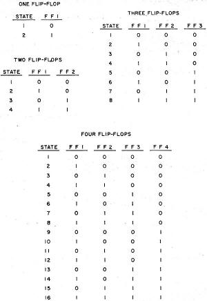
Fig. 2 - All possible states of divider with up to 4 FF's.

Fig. 3 - Circuit and operation of synchronous n = 3 divider.
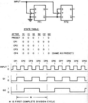
Fig. 4 - Synchronous n = 4 divider with an n = 2 output.

Fig. 5 - Circuit and operation of synchronous n = 5 divider.

Fig. 6 - Circuit and operation of synchronous n = 6 divider.

Fig. 7 - Circuit and operation of synchronous n = 7 divider.

Fig. 8 - Synchronous n = 8 divider with synchronous n =
2,4 outputs.

Fig. 9 - Circuit and operation of synchronous n = 9 divider.

Fig. 10 - Arrangement employed for synchronous n = 10 divider
with its counting sequence chosen for easy decoding.
The frequency divider has a division ration if its output waveform passes through
one complete cycle as its input waveform passes through n complete cycles. The number
of FF's required in a particular divider is determined by the desired division ratio.
The highest possible division ratio for a given number of FF's is 2x
where x is the number of FF's in the divider. Thus, one FF is needed to divide by
two; two FF's are needed to divide by three or four; three FF's are needed to divide
by five, six, seven, or eight, etc.
The signal input connected to T (pin 2 of the particular C discussed last month
in Part 1) of each FF in the divider will be either the incoming CP or the output
of a preceding FF. If T of each FF is connected to the incoming CP, the divider
is a synchronous divider. If the incoming CP is connected to T of the first FF only,
and T of the second FF is connected to the output (Q or
Q) of the first FF, etc., then the divider is called
an asynchronous divider.
The FF propagation delays in the asynchronous divider are cumulative and the
time between CP's must be sufficient to allow each FF in the divider string to change
state. In general, no more than about six 9923 JK FF's should be used in anyone
asynchronous divider intended to operate at an input frequency of 2 MHz. All FF's
in the synchronous divider are triggered simultaneously and the time delay between
the CP and the resulting change in divider output is equal to the propagation delay
time of one FF rather than the combined propagation delays of a string of FF's.
Synchronous dividers should always be used when the divider input and output waveforms
must be in synchronism.
The control inputs 5 and C (pins 1 and 3 respectively) of a particular FF are
connected to ground (0 level), + VCC (1 level), or the outputs of other
FF's either directly or via gates. The level applied to S, the level applied to
C, and the "present" FF state determine the state of the FF after the next CP or
1-to-0 transition of a preceding FF. Fig. 1 is an expanded version of the truth
table in Fig. 7 of Part 1. It lists all possible combinations of S, C, and
JK FF states that might exist before the arrival of a CP and gives the FF state
that will then result after the arrival of the CP. Keep in mind that a CP is simply
a 1-to-0 transition at T (pin 2) and that the state of the FF is the level at Q
(pin 7).
If Preset (pin 6) of all the 9923 FF's in a divider are connected together, all
of the FF's will be forced to the 0 state (output Q at the 0 level) when this "preset
line" is momentarily connected to VCC (+3.6 V d.c.). This technique provides
a convenient starting point for the dividing action both in the operating circuit
and on paper.
It is customary to define the instantaneous state of the divider as the states
of the FF's in the divider written in some logical order. Thus, if the divider is
made up of four FF's labeled FF1, FF2, FF3, and FF4, and FF states are 1, 0, 1,
and 1, respectively, then the state of the divider is 1011. Since each FF has two
states (1 and 0), the number of possible divider states is 2x where x is the number
of FF's in the divider. All possible states of a divider having 1, 2, 3, or 4 FF's
are tabulated in Fig. 2.
Circuit waveforms for the more complex dividers are determined from a state table.
The state table is a CP-by-CP tabulation of the levels at S, C, and Q of every FF
in the divider. It is most convenient to assume that the divider starts from the
Preset state (i.e., all Q's at 0). The levels of each FF S and C input are then
determined from the divider schematic. Knowing S, C, and Q, the FF states after
the first CP may then be determined from Fig. 1. The "new" S and C levels are
determined and the FF states after the second CP are determined. This process is
continued until the state table begins to repeat itself, indicating that one complete
division cycle has occurred.
The completed state table should be compared with Fig. 2 to determine which
(if any) of the possible divider states in Fig. 2 do not appear in the state
table. Additional state tables are then constructed using each of these "unused"
divider states as the initial starting point in order to determine if the divider
will recover and divide by the desired ratio. If it does not, two courses of action
are available: redesign the divider, or make provisions for Presetting the divider.
There may be more than one circuit that will yield a particular division ratio.
The circuit finally chosen will usually be the one that uses the fewest components
or provides the most desirable output waveform for the particular application. It
frequently happens that more than one division ratio can be obtained from a single
divider. For example, a divide-by-ten circuit may be able to simultaneously deliver
a divide-by-two or divide-by-five output from some point in the circuit.
The circuits to follow are drawn using the logic symbols of the IC devices. Refer
to Fig. 8 in Part 1 for the actual Fairchild IC pin numbers. Although not shown,
pin 4 of each IC is grounded and pin 8 of each IC is connected to VCC
(+3.6 V d.c.). If the Preset feature of the JK FF's is employed, then connect pin
6 of each of the FF's together and connect this to VCC through a normally
open momentary switch.
Either Q or Q of any FF in the divider may be
chosen as the divider output (s). For a given FF, the more lightly loaded of the
two output terminals is usually used, although this is not mandatory as long as
the output drive factor of the FF is not exceeded.
In the figures that follow, the input signal is drawn as a square wave only for
purposes of illustration. The input waveform may be of any shape as long as the
fall-time is small enough to be accepted by the FF's as a clock pulse. The area
marked "first complete division cycle" is the waveform that will repeat with every
n clock pulse.
Dividing by Two
The simplest possible frequency divider is an n =2 divider made from a single
JK FF. If the S and C inputs are both (permanently) at 0, the FF changes state with
each CP. If the FF is initially in the 0 state, it will change to the 1 state when
the first CP arrives. When the second CP arrives, the FF returns to the 0 state.
On the third CP, the FF changes back to the 1 state, completing the output cycle.
The FF state alternates with each consecutive CP and the output frequency is one-half
the input frequency - or the output waveform period is twice the input waveform
period.
Dividing by Three
Then n = 3 divider in Fig. 3 is a synchronous divider - the CP is applied
simultaneously to the T input of both FF's. The input load factor is 10 since each
FF has an input load factor of 5.
The state table for the divider of Fig. 3 is constructed as follows:
a. After Preset, Q1 (output Q of FF1) and Q2 (output Q of FF2) are both 0. These
0's are entered in the Q1 and Q2 columns on the Preset line of the table.
b. Now that Q1 and Q2 are known, all of the S and C levels may be determined
directly from the divider schematic: S1 = Q2 =1;
C1 = 0; S2 = 0; and C2 = Q1 = 1. These levels are
entered in their appropriate columns on the Preset line of the table.
c. The levels entered on the Preset line of the table are the levels at S, C,
and Q that now exist before the arrival of the first CP. The levels at Q1 and Q2
after the arrival of the first CP are obtained directly from Fig. 1: Q1 = 1
and Q2 = 0. These levels for Q1 and Q2 are entered on the CP1 line of the table.
d. Now that Q1 and Q2 after CP1 are known, the S and C levels after CP1 are determined:
S1 = Q2 = 1; C1 = 0; S2 = 0; and C2 =
Q1 = 0. These levels are entered in their appropriate
columns on the CP1 line of the table.
e. Continuing in this manner, after CP2: Q1 = 1; and Q2 = 1. Also, S1 = 0; C1
= 0; S2 = 0; and C2 = 0.
f. After CP3: Q1 = 0 and Q2 = 0. Also S1 = 1; C1 = 0; S2 = 0; and C2 = 1. This
divider state is identical to the Preset state; therefore, the cycle will be repetitive.
If a CP4 line were added to the table, it would look exactly the same as the
CP1 line; a CP5 line would be the same as the CP2 line; a CP6 line would be the
same as the CP3 line, a CP7 line would be the same as the CP1 line, etc. The waveforms
in Fig. 3 are constructed directly from the information in the state table.
The three states of the divider are 00, 10, and 11. Comparing these states with
Fig. 2 reveals that the 01 state is missing from the divider operating sequence.
A state table using an initial state (U1 ) of 01 demonstrates that the divider will
perform exactly the same as when the initial state is 00; the divider state one
CP after the initial state is the same in both cases and the waveforms are identical.
Bear in mind that if the Preset function is used as explained earlier, this evaluation
of the divider recovery from an "unused" state is unnecessary. It is explained in
this section only to demonstrate the technique.
Dividing by Four
The simplest means of dividing by four is to divide by two twice. The output
of the first divider is at one-half the input frequency and is connected to the
input of the second divider. The second divider divides the output frequency of
the first divider by two and the resulting output frequency is one-fourth the input
frequency to the first divider. Simultaneous n = 2 and n = 4 outputs may be obtained
from this divider. The n = 2 output is synchronous, but the n = 4 output is asynchronous
since it is delayed from the input CP by the sum of the propagation delays of both
flip-flops.
The synchronous divider in Fig. 4 also provides simultaneous n = 2 and n
= 4 outputs. The synchronous n = 4 output is obtained at the expense of slightly
increased circuit complexity and a larger input load factor.
Dividing by Five, Six, Seven, Eight & Nine
Fig. 5 is a n = 5 divider. All outputs are synchronous and have the same
waveshape, but are time-displaced from one another. The circuit will recover from
its unused states so the use of the Preset function is optional.
Fig. 6 is a simple synchronous n = 6 divider. In addition to the n = 6 output
from FF3, n = 3 outputs are available from either FF1 or FF2. The divider has two
unused states and will recover from either. A division ratio of six may also be
obtained by dividing by two and then by three (or vice versa).
A synchronous n = 7 divider appears in Fig. 7. The divider has one unused
state and will recover on the next CP. An asynchronous n = 7 divider can be constructed
and requires one less gate than the synchronous divider.
An asynchronous n = 8 divider is most easily assembled by cascading three n =
2 dividers. A synchronous divider is shown in Fig. 8. Regardless of the method
used, n = 2 and n = 4 outputs will also be available and there are no unused states.
Fig. 9 is a synchronous n = 9 divider. It has seven unused states and will
recover from each. Cascading two n = 3 dividers will provide an asynchronous n =
9 output and a synchronous n = 3 output.
Dividing by Ten
Many n = 10 dividers have been devised due to their popularity in dividing and
counting applications. An asynchronous n = 10 divider could be built from an n =
2 divider and an n = 5 divider. A synchronous n = 2 or n = 5 output (depending on
which divider is connected to the incoming CP) would also be available.
The synchronous n = 10 divider in Fig. 10 operates in the so-called "shift
mode." Although this divider requires one additional FF and provides only n = 10
outputs, it is particularly useful in counting applications as we shall see later.
The divider has 22 unused states - an ideal opportunity to utilize the Preset function.
Practical Systems
Typical frequency-divider systems consist of one or more divider stages cascaded
to provide the desired division ratios and outputs. A common application is that
of cascading several n = 10 dividers to divide a 1-MHz or 100-kHz signal down to
10 kHz, 1 kHz, etc. Buffers are used between divider stages when an increase in
drive level is required. They should also be provided on the output lines if external
circuit loading is appreciable.
Whatever the ultimate application, the first problem encountered is usually that
of converting the input waveform to a fast-fall-time pulse to act as a clock pulse
for the dividers. The circuit of Fig. 11 will accept any input waveform and
has been used by the author to drive some of the dividers in this article at frequencies
in excess of 10 MHz.
The circuit functions like a low-hysteresis Schmitt trigger that switches at
a threshold voltage of about 0.9 V d.c. D1 may be any signal diode - its only function
is to protect IC1 from negative-going inputs. Naturally, the voltage at pin 1 of
IC1 should not exceed 3.6 volts in the positive direction. The choice of C1 is based
on the input signal amplitude and frequency. For inputs of 100 kHz and over, a 0.1-μF
capacitor is adequate. If R4 is set midway between the two trigger levels, the circuit
will operate reliably on a.c. inputs well under 100 m V peak-to-peak. If R3 and
R4 are omitted, then the minimum a.c. input must be on the order of 2 volts peak-to-peak.
The power supply requires no particular attention other than assuring that its
output voltage is low in ripple and transient-free. A full-wave rectifier followed
by a filter capacitance of 25,000 μF or more will be adequate on both counts.
An allowance of about 25 mA d.c. per IC will suffice for estimating total d.c. current
requirements.
Fig. 11. Circuit for generating clock pulses from any input. Output can
drive the equivalent of 16 flip-flop "T" inputs.
Fig. 12. Decoder for the n = 10 divider shown in Fig. 10.
Frequency Counters
Although the term "frequency divider" has been used throughout this article,
the frequency dividers are actually repetitive counters. When the input CP's to
the counter are regular and periodic, frequency division is obtained as a by-product
of the repetitive counting operation. In frequency-dividing applications, one is
interested in the time-varying waveforms present at the FF outputs during the counting
operation; in counting applications, one is interested in the states of the individual
FF's at a particular instant of time.
In order for the counter to be of any real value, information on the FF states
must be presented in some usable form. Typically a lamp-driver/lamp circuit is used.
The lamp driver is designed so that the lamp illuminates when the lamp driver input
is at the 1 level and extinguishes when it is at the 0 level.
Decade Counters
The decade counter is designed to display the number of clock pulses counted
in numbers from 0 to 9. On the 10th CP the counter resets to 0 and delivers an output
pulse. If this pulse is connected to the input of a second decade counter, the display
of the second counter advances one count for every ten counts of the first decade
counter. Connected in this manner, one decade counter counts from 0 to 9 clock pulses,
two decade counters count from 0 to 99 clock pulses, three decade counters can count
up to 999 clock pulses, etc.
A decade counter is designed around an n = 10 divider. Since the divider state
is different for each successive CP, the lamp responses can be related to the divider
states through appropriate decoding techniques. Any n = 10 divider can be decoded,
but the divider of Fig. 10 is ideally suited since it can be completely decoded
using only ten two-input gates.
A decoder for the Fig. 10 divider is shown in Fig. 12. The inputs Q1
through Q5 are connected to the corresponding FF outputs of Fig 10. When the divider/counter
is Preset (all FF outputs at the 0 level) only the "0" decoded output is at the
1 level. After the first CP only the ''1'' decoded output is at the 1 level. After
the second CP only the "2" decoded output is at the 1 level. After the ninth CP
only the "9" decoded output and output X are at the 1 level. Coincident with the
tenth CP output X switches to the 0 level providing a CP to drive a second decade
counter.
Posted August 16, 2024
(updated from original
post on 5/23/2017)
|