|
January 1963 Electronics World
 Table
of Contents
Table
of Contents
Wax nostalgic about and learn from the history of early electronics. See articles
from
Electronics World, published May 1959
- December 1971. All copyrights hereby acknowledged.
|
The basics of power transistor
specification and selection have not changed much since they became widely commercially
available in the 1960s. Although available package shapes, power handling, cutoff
frequencies, and other parameter options have been greatly expanded, still the most
important aspect is not just selecting a power transistor but properly mounting
it to ensure that the rated heat dissipation capacity will be realized. That can
mean thermal grease, a heat sink, a fan, and even ducting or water cooling. This 1963
Electronics World magazine article touches on some of those considerations
and how to effectively deal with them.
Power Transistor Specifications
 By John R. Gyorki/ Burroughs Corporation
Discussion of important mechanical, electrical, and thermal characteristics to
familiarize the technician with several basic transistor limits.
Although a great number of power transistor specifications can be devised (and
the number seems endless), a few of the more common and important mechanical, electrical,
and thermal characteristics will be discussed. Without a doubt, the sophisticated
power transistor as we know it today would not exist if it were not for the absolute
control of a myriad of fine characteristics during manufacturing and sorting. However,
we are concerned only with the ratings that decide how we can best keep a device
operating at its highest efficiency.
Mechanical Characteristics
One of the industry's most common power transistor package styles is the diamond
base, also commonly known as the "TO-3." It has straight pins that can be plugged
into a suitable socket (through a heat sink or radiator) and is usable with emitter
currents of ten amperes or less. Socket connections, however, are not satisfactory
connections and develop voltage drops; just as voltage drops across a resistance.
Also, excessive heating losses occur when currents above the ten-ampere rating are
used. Therefore, we must utilize a more substantial type of transistor.
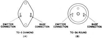
Fig. 1 - Two common power transistor basing arrangements.
In both cases collector is internally connected to case.
Another equally popular style is the round type, "TO-36." It is generally used
for emitter currents of 15 amperes and above. Two straight pins are used for the
base and emitter connections with holes in them for soldering or they are available
with tinned leads welded directly to short emitter and base studs.
In both types, the collector is mechanically and electrically fastened to the
transistor case. The case serves as the collector terminal and thermal radiator
connection. This is done since the collector junction becomes very warm during operation.
The emitter and base leads usually can be identified by observing an "E" and a "B"
stamped on the transistor case near the respective leads. However, this is not always
the situation, so a basing diagram for the particular transistor being used should
be consulted. Fig. 1 shows the typical lead arrangement for both styles.
The diamond package is held in place by a 6-32 screw inserted through each hole
in the opposite corners of the heavy mounting base. The round style is mounted by
a single threaded stud projecting outward from the bottom. A 10-32 nut and lock
washer terminal is used to secure it in place. The recommended torque on the TO-36
mounting stud is 12 inch-pounds; no more should be used. Appropriate insulating
washers are often used at this time to electrically insulate the transistor from
the heat sink. This will be discussed more fully under thermal conditions.
Transistors are not mechanically shockproof in themselves. However, their rigid
construction makes them suitable for use in rugged type equipment. They are hermetically
sealed with a metal cap, either hot or cold welded to the mounting base. This excludes
moisture and light, both of which can degrade the quality of the device.
Electrical Characteristics
Leakage Current: Collector cut-off currents are simply other words used for discussing
inherent leakage currents associated with the collector while the base and emitter
are held to pre-determined conditions.
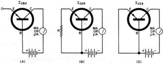
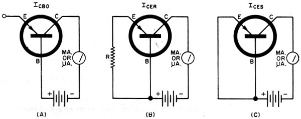
Fig. 2 - Circuits for measuring leakage currents of transistors.
One of the most important collector leakage currents is ICBO or more
commonly, ICO. See Fig 2A. It is a leakage current from collector to
base with the emitter open-circuited and is critical because it is most susceptible
to temperature variations. Since power transistors operate with high junction temperatures,
changes in ICO could greatly affect the stability of the transistor and
circuit. ICO can easily be demonstrated by constructing the circuit of
Fig. 2A. Heat from your hand or a lighted match brought near the transistor
will change the indicated leakage current enough to be quite obvious.
Leakage current from collector to emitter with the base circuit open is termed
ICEO. This is a condition that could be expected in switching applications;
the base open and the collector supply voltage present across the collector and
emitter. In better switching circuits, however, the base circuit is not entirely
open. It is usually reverse-biased or connected to the emitter by a low value resistor.
Two other collector leakage currents are ICER, with a specified resistor
from base to emitter, and ICES, with the base shorted to the emitter.
They, as well as ICBO, are measured with the conventional reverse-bias
voltage from collector to base. See Figs. 2B and 2C.
These leakage currents vary from a few microamperes to a few milliamperes, depending
on the specific transistor type. They are among the most critical power transistor
ratings and should be kept as low as possible. Increased leakage current causes
a rise in junction temperature; a rise in temperature creates more leakage current.
This condition is called thermal runaway and, if not controlled, could end in the
destruction of the transistor. Outside factors which generally determine the over-all
stability are controlled by the circuit designer.
Voltage Breakdown: Collector breakdown voltage is that reverse voltage applied
between collector and emitter where the collector current begins to avalanche and
the collector current becomes independent of collector voltage. This constitutes
a group of breakdown voltages where the base and emitter are held to various constants.
One such voltage is BVCBO, the reverse breakdown voltage between collector
and base with the emitter open. See Fig. 3A.
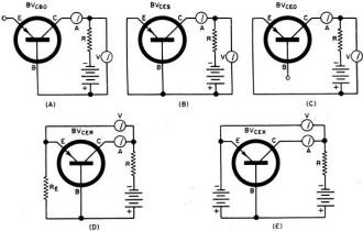
Fig. 3 - The various breakdown-voltage measurements are
depicted.
Two other breakdown voltages are BVCES, base shorted to emitter, and
BVCEO, the base open-circuited. Refer to Figs. 3B and 3C. These are important
considerations when circuits with inductive loads are used. During transient voltage
peaks the actual instantaneous voltage present between collector and emitter may
be very much higher than the supply. It is at this time especially we do not want
the collector-to-emitter voltage rating exceeded.
Another breakdown voltage is BVCER. This arrangement has a specified
resistor between base and emitter (usually around 10 ohms). See Fig. 3D.
BVCEX is the reverse breakdown voltage between collector and emitter
with a small reverse bias between the base and emitter of 0.1 volt or more. This
constitutes the absolute maximum surge voltage limit that the transistor can tolerate.
Steady-state voltages are not used to measure these breakdown voltages (as may
be implied from the diagrams) because of the excessive junction heating which could
destroy the transistor before final results were tabulated. Rather, a sweep method
is used, employing an oscilloscope and a sine-wave generator where collector voltage
versus collector current can be observed and the breakdown curve clearly indicated
without undue junction heating. (See "Motorola Power Transistor Handbook," First
Edition, Chapter VIII "Transistor Testing," page 159.)
Collector saturation voltage, VCE (sat), is that small voltage appearing
between collector and emitter with such large base drive applied (forward bias)
that any further increase in base current will not change the collector current
appreciably. In other words, this is where further collector injection (by the base)
brings to a halt the further increase of collector current. Current gain is no longer
considered existent at these high current levels. Saturation voltage ratings of
most transistors are measured with a specified value of collector and base current.
Current Gain: Transistor current gain, beta, is the ratio of
a change in collector current to a change in base current. This is the actual usable
current amplification rating of a particular transistor. Current gain specifications
in power transistors are generally given a range of values for a specific transistor.
These values are known as "large-signal current gain" and are primarily used over
the mean values of maximum collector currents. "Small-signal current gains" are
sometimes specified for medium- and high-power transistors, but more generally are
considered a special case, since only a very small portion of the allowable collector
current is actually used. That is, the current gain of a power transistor is much
higher at low collector current levels than at high collector currents.
Cut-Off Frequency: Current gain frequency cut-off, fae.
(common emitter), is that frequency where the small-signal current gain of the transistor
is 3-db down from some pre-determined value specified at a particular frequency.
This means that the current gain at fae is 0.707 of the value specified
at some reference frequency (usually 1 kc.). The actual cut-off frequency is usually
10 kc. for most common power transistors.
Other Characteristics: There are a few other normal operating
characteristics concerning voltage and current that are important and should be
considered.
Maximum emitter current is a common rating and means just that; the maximum emitter
current that can flow before permanently damaging the device. This is probably one
of the first practical operating ratings considered for either replacement or new
design purposes.
Collector-to-emitter voltage is usually specified with the base shorted to the
emitter or with the base open-circuited. In either case, the rating is specified
with a certain value of collector current.
Collector diode voltage, VCB (voltage, collector-to-base) is indicated
with a value of emitter-to-base voltage. The actual circuit supply voltage should
be less than the collector diode or collector-to-emitter voltage ratings.
Base current is usually given as a continuous value or a maximum value. This
base current rating should not be exceeded or the junction will overheat and destroy
the transistor.
Power and Thermal Ratings
Power dissipation and junction temperature rise are directly related since the
rise in junction temperature is caused by power being dissipated in the junction.
The maximum allowable junction temperature of germanium power transistors is 100°C
(212°F). Any higher temperatures will soften and finally melt the germanium.
The average power dissipation is equal to the emitter current multiplied by the
collector-to-emitter voltage. This will yield a hyperbolic curve that can be found
on typical output characteristics curves. The transistor circuit load line, incidentally,
must stay under this curve to insure reliable operation of the transistor and keep
excessive power dissipation in the junction down to a safe level.
Thermal conductivity is the ability of a material to transmit heat along or through
itself. The heat conductivity path from the transistor collector junction to the
ambient air must have as little heat resistance as possible. Since the junction
of an operating transistor heats and the temperature of the ambient is normally
less than the transistor junction temperature, it is desirable to have the junction
heat radiating into the surrounding air and allow the junction to approach the temperature
of the ambient. If the heat transfer path from the transistor junction to the air
were 100% efficient, the junction temperature would be the ambient temperature.
However, this is not practically possible. Between the transistor junction and the
ambient air we find the connection between the junction and the case, case and insulator,
insulator and heat sink, heat sink and air; all of which total up to an opposition
in the path from junction to air. These obstacles are known separately as thermal
resistance. Each different thermal resistance has a unique coefficient number. The
coefficient of thermal resistance is expressed as a temperature in degrees centigrade
per watt of dissipation. Due to these resistances, there will always appear a temperature
differential between transistor junction and ambient. This temperature differential
must be reduced to as low a value as possible.
The actual amount of temperature difference depends upon the amount of power
the transistor junction is dissipating. We add up the individual thermal resistances,
multiply the total thermal resistance by the power being dissipated by the transistor
junction (P = EC x IC and add the results to the ambient temperature.
This gives us the transistor junction temperature. If the junction temperature just
calculated is over the maximum allowable rating for the transistor, one or more
factors will have to be reconsidered. We can lower the collector current and voltage
to reduce power dissipation (and consequently the stage output power) or, perhaps,
we might lower the ambient temperature. This could be done by adding a fan for air
circulation or by relocating the assembly in a cooler environment. Any one of the
thermal resistances may be lowered to accomplish the same end, but this may be a
little more difficult to do. With the new values determined, the junction temperature
must be re-calculated. A useful formula for this is
TJ = PD (θJC + θCS + θSA)
+TA where: TJ = junction temperature in degrees C, PD
= power dissipation in watts (collector current x collector voltage), θJC
= transistor thermal resistance in degrees C/watt (junction to case), θCS
= insulator thermal resistance in degrees C/watt (case to heat sink), θSA
= heat sink thermal resistance in degrees C/watt (heat sink to ambient), and TA
= ambient temperature in degrees centigrade.
Insulators used are mica, Teflon, or anodized aluminum. They are used only where
the collector must be electrically insulated from the heat sink, but not thermally,
Silicone grease applied in small amounts between the transistor and heat sink (and
insulator when used) can reduce thermal resistance even more, enhancing total heat
dissipation. Teflon has the highest thermal resistance with mica second and anodized
aluminum the lowest. Teflon and mica are not as mechanically durable as anodized
aluminum, but scratches through the anodized coat on both sides of the aluminum
can electrically short the transistor to the heat sink. Silicone-coated mica insulators
seem to be the most popular choice at the present time in the industry at large.
However, no insulator at all, with silicone grease between the transistor and heat
sink, is the best possible situation.
The maximum amount of heat transfer takes place in the immediate vicinity of
the mounting studs on the TO-36 package and around the holding screws on the TO-3
package. The mounting surface is smooth and made of copper or is plated with another
metal, such as nickel, to enhance thermal conductivity. In general, securing a heat
radiator to the cap of the transistor affords little or no heat dissipation. The
transistor mounting base surface is the only reliable area for connection to a heat
sink.
Conclusion
The many power transistor specifications that are required in the manufacture
of transistors are not necessarily the same specifications required for field technicians.
Once the transistorized equipment is designed and used, the technician need only
be aware of certain practical and general precautions in the replacement of transistors,
that is, if he does not have a direct replacement, a substitute may be used. In
such a case, a knowledge of a few transistor characteristics will assist him in
making an intelligent guess as to a proper replacement and insure operation of equipment.