|
|
|||||||||
| Software: RF Cascade Workbook | RF Symbols for Office | RF Symbols & Stencils for Visio | Espresso Workbook | ||||||||||
|
|||||||||||||||||||||||||||||||
  |
  |
||||||||||||||||||||||||||||||
|
Please Support RF Cafe by purchasing my ridiculously low-priced products, all of which I created. RF & Electronics Symbols for Visio RF & Electronics Symbols for Office RF & Electronics Stencils for Visio T-Shirts, Mugs, Cups, Ball Caps, Mouse Pads These Are Available for Free |
|||||||||||||||||||||||||||||||

"Printed Wiring" Techniques for the Experimenter
August 1956 Popular Electronics

|
August 1956 Popular Electronics  Table of Contents Table of Contents
Wax nostalgic about and learn from the history of early electronics. See articles from Popular Electronics, published October 1954 - April 1985. All copyrights are hereby acknowledged. |
In part one of a two-part article, Popular Electronics magazine presents some of the inner workings of what at the time was a fledgling industry - printed circuit board manufacturing. In 1956, when this piece appeared, a large percentage of electronics assemblies were still being wired in a point-to-point manner where resistors, capacitors, inductors, tubes, and cables were soldered directly to terminals either on special blocks or on tube sockets. The process was heavily labor intensive and prone to miswirings. High volume production was nearly impossible prior to printed wiring boards (PWBs). Bell Telephone Labs was an early adopter and driver of the technology. A good example of an early telephone PWB can be seen in the 1970s vintage Snoopy telephone that I reconditioned a while back. Note the rat's nest of wires going to the network terminal block. Here is Part 2.
Check out "How to Etch Professional Printed Circuit Boards" in the March 1966 Popular Electronics.
"Printed Wiring" Techniques for the Experimenter
Part I of two-part series discusses methods of printed wiring and tells how to make an etched circuit board
Courtesy of Bell Telephone Labs.
Radio receiver "wired" without hookup wire! An audio amplifier, assembled without terminal strips! A television receiver with hundreds of soldered connections ... but all made without a soldering iron!
Far-fetched? No, All of these production miracles may occur as a matter of course when a manufacturer substitutes "printed" wiring methods for conventional hand wiring, Since the elimination of hand wiring can cut labor production costs as much as 50%, manufacturers have a sound economic reason for using such methods.
But the savings in labor costs is not the only reason for going to printed wiring. The finished equipment may be more compact, work better, and require fewer adjustments. Finally, since every unit is wired exactly alike, wiring errors are virtually eliminated, "rejects" are minimized, and inspection time and costs are reduced.
Methods of Printed Wiring. The general term "printed wiring" is used to describe any electrical or conductive pattern reproduced on an insulating base, although technically the term applies only to wiring and circuits reproduced with the aid of printing techniques ... that is, using conductive inks printed in the desired pattern. Commercially, printed wiring may be of two general forms - "deposit" and "stripped."
In making up a printed·-circuit layout, you start with a schematic wiring diagram of the project you plan to assemble, redrawing it until you have eliminated all circuit wiring crossovers. See text for more details.
Typical etched circuit layout on cross-section paper. Drawing should be made to full-size scale.
Clean the copper-clad phenolic wiring board of dirt and tarnish prior to applying the resist.
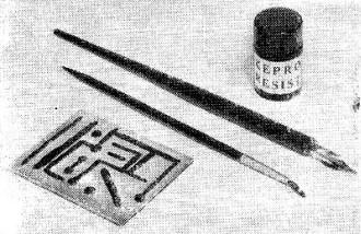
Ink resist is applied with brush and pen. Only those parts covered will remain after etching.
Scotch electrical tape may be used as a tape resist. Circles are cut out with a paper punch.
If a "deposit" method is used, the conductive pattern is applied to the insulating base plate. Typical "deposit" methods include printing with metallic inks, spraying liquid metal onto the base through a stencil, and pressing a metallic foil pattern into a plastic base, using a heated die.
Where a "stripping" method is used, the insulated base is covered with the conducting material. The desired pattern is applied to the surface, and the excess conductor "stripped" away. The more popular "stripping" techniques include etching and embossing.
Use of printed wiring methods offers advantages to the home experimenter, student, or gadgeteer making up a single circuit as well as to the manufacturer producing thousands of units. When reasonable skill is acquired through practice, it is often possible to layout, produce and assemble a piece of equipment using printed wiring in less time than it takes to make up the same circuit using conventional wiring techniques ... and with the final equipment much more "professional" in appearance, more compact, and likely to work better.
With the advantages to the experimenter in mind, several manufacturers are offering printed-circuit kits. These kits include all the materials necessary to make up etched circuit boards. Basic printed wiring techniques have been described briefly in past issues of Pop'tronics in regard to specific projects. See H. J. Carter's, "Making an Etched Preamp" (November, 1955, p. 87), and Paul F. Runge's "Printed Circuitry for R/C" (August, 1955, p. 74). But now we'll discuss these techniques in detail and show how you can apply printed wiring methods to virtually any project that you wish to assemble.
Of the various printed wiring techniques used industrially, the techniques of "etching" and "painting" are best suited to home use. Of the two, etching is by far the most popular and is, in fact, the most widely used commercial technique. The majority of printed-circuit kits utilize etching techniques.
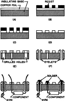
Making Etched Circuits. The basic. steps in producing an etched wiring board and assembling a circuit are illustrated in Fig. 1 (p. 62). The raw material is a laminated ,board consisting of an insulating base with a layer of metal foil bonded to its surface. The foil may be on either one or both sides. In most work, a copper-foil clad laminated paper-base phenolic Is used.
You can make up your own etched circuit boards by following these essential steps - plus the additional steps of making up the original circuit pattern layout and transferring the layout to the board. Follow the procedure detailed below:
Step 1 - Making a Layout. Start with the schematic wiring diagram of the project you plan to assemble. Redraw the schematic one or more times, trying to eliminate all circuit wiring crossovers. When you have a tentative circuit, gather the components you plan to use and make a full-size scale drawing of the final circuit. Locate components where they will serve to bypass conductor crossovers which are not easily eliminated. Individual leads or "wires" should have a thickness of at least 1/32", with the spacing between adjacent conductors not less than 1/32". Thicker leads may be used if desired, and you may find it easier to work with 1/16"- or even 1/8"-wide conductors on the first few boards you make up.
Where components are to be mounted or leads attached to the board, draw small circles. Entire patches of foil conductor may be used for shielding, although it is generally best to "break up" solid areas with diagonal bars. The spacing between adjacent bars may approximate or be slightly greater than the width of the bars. Where 90° turns are made, the conductor may follow a smooth curve or make a sharp bend, as preferred. Where eyelets are to be used, plan on holes large enough to accommodate them. Use slightly smaller holes when leads are to be attached directly to the copper foil.
In general, component and wiring leads can be soldered directly to the copper foil for permanent connections, but if the leads may be removed often, plan on using copper or brass eyelets at such points. Space component mounting holes for the actual parts you plan to use. If the components are to be mounted by their leads (resistors, capacitors, and small coils are generally mounted in this fashion), space the mounting holes with the thought of using a gradual bend in the component leads instead of a sharp bend close to the body ... sharp bends may cause the leads to break off or can place an undue strain on the component. You will find that cross-section (graph) paper is useful for making up the scale wiring layout.
A "typical" printed wiring layout is illustrated in Fig. 2. This layout has been designed to illustrate important points to remember when making up your own layouts and it does not represent a specific circuit.
Upon completing a circuit wiring layout, check and double-check for errors. While still in the layout stage, an error may be corrected simply by erasing and redrawing the layout ... but once the board is etched, it may be necessary to make up an entire new board to correct mistakes.
Step 2 - Preparing the Board. The copper-clad phenolic board and other materials you'll need may be purchased individually or in "kits." (See list of suppliers on page 62.) At the beginning, however, you'll find it best to purchase a complete "kit" of materials. Once you've gained a little experience in making up circuit boards, you can purchase individual items in the quantities needed.
Fig. 1 - In the commercial production of etched circuit boards, the plain metal clad board shown at (A) is covered with a special material which resists chemical action. This "resist" is applied in the pattern of the desired final circuit, as shown at (B), using photographic, plating, spraying, stenciling, or printing techniques. With the resist applied, the foil-clad board is placed in a chemical etchant which attacks and eats (etches) away all unprotected metal, leaving only the foil pattern protected by the resist (C). After that, the resist is removed, exposing the bare metal foil (D). Machining is next (E), with mounting and wiring holes drilled or punched at appropriate places in the board. Metal eyelets, if used, are now mounted in the board (F). With step (F), the wiring board itself is completed. To complete the circuit, electrical components are mounted on the back of the board by passing their leads through appropriate holes in the board (G). Finally, the board is soldered and excess lead lengths cut off, resulting in the completed circuit shown at (H). In production work, the entire board is generally soldered in one operation by dipping it into a "pot" of solder - with the operation called, appropriately, "dip soldering." Thus, hundreds of soldered connections may be made at one time without a soldering iron!
Depending on the circuit layout, use either single-sided (single-clad) or double-clad boards. But until you gain experience, you'll find it best to stick to simple layouts and single-clad board.
Cut a piece of the copper-clad board to fit your circuit layout, using a fine-toothed hacksaw, a jigsaw, or a scroll saw. Cut from the copper side, and back up the thin phenolic board with a piece of hardboard or plywood. If any large holes or cutouts are needed (for tube sockets, for example), they should be cut at this time. Use a hole saw or "flying bar" cutter for cutting large round holes ... not a conventional chassis punch, which may crack the board. Only the large holes and cutouts are made at this time ... smaller holes are drilled after the board is etched.
With the board cut to size and rough machine work completed, clean the copper surface of dirt and tarnish, and roughen it slightly to permit the etchant to get a better "bite" on the foil. You can do this by scrubbing the surface with a stiff brush dipped in powdered pumice stone (check your local hardware dealer) or, if pumice stone is unavailable, by using an abrasive household cleanser. Sprinkle the household cleanser lightly on the foil and scour vigorously with a slightly dampened cloth. With the surface properly prepared, the copper should be bright and shiny, and should have many small scratches ... visible when the foil is examined through a small magnifying glass. Then you should rinse and dry the prepared board.
Step 3 - Transferring Layout. First, obtain a few sheets of "pencil" carbon paper from your local stationer or office supply store. Cut a piece to fit your circuit board and attach the carbon paper and your scale wiring layout to the board with Scotch tape. Make sure the layout cannot shift its position. Finally, using a moderately hard pencil, trace the layout onto the copper foil.
Locate small mounting holes by pricking the copper right through the layout and tracing carbon, using a small center punch or a sharp scribe. Use hand pressure or a very light hammer tap when locating these holes to avoid cracking the board. Back up the board with a solid piece of hardboard or wood. And double-check your tracing before removing the layout sheet and carbon paper.
Step 4 - Applying the Resist. With the circuit layout transferred to the copper-clad board, the acid "resist" may be applied. For experimental "single-shot" circuits, two types of resist are popular: (1) ink resist and (2) tape resist.
Ink resist is an asphalt-based acid-resistant paint or ink. It is supplied as a part of most printed-circuit kits but is also available from many art supply houses. Apply ink resist to the copper foil using a small ruling pen, a small brush, or a "Speedball" pen. Cover all parts of the layout, for only those parts of the copper foil covered by the ink will remain after etching. Allow the ink to dry.
Ordinary plastic-base Scotch electrical tape makes an excellent tape resist. It is furnished in some kits. Narrow strips may be cut from the standard width using an "Xacto" knife, a razor blade, scalpel, or similar tool. Small circles, for terminal connections, can be punched out with a small hand paper punch. The tape is simply applied to the copper foil to cover the traced layout pattern, then burnished down with a smooth, hard tool. A good burnishing tool can be made quite easily by rounding the end of a wooden dowel peg.
Double-check the circuit board after applying the resist. Compare it to the original layout. If you find you've made an error, correct it. Ink resist may be removed by using a hard (ink) eraser. Tape resist is simply peeled off. Reapply the resist to correct the error.
Fig. 2 - A "typical" board which illustrates the important points that you should remember in making up your own printed-circuit layout. It does not represent specific circuit.
Posted April 18, 2022
(updated from original post on 10/19/2016)

Copyright: 1996 - 2026 |
About RF Cafe RF Cafe began life in 1996 as "RF Tools" in an AOL screen name web space totaling 2 MB. Its primary purpose was to provide me with ready access to commonly needed formulas and reference material while performing my work as an RF system and circuit design engineer. The World Wide Web (Internet) was largely an unknown entity at the time and bandwidth was a scarce commodity. Dial-up modems blazed along at 14.4 kbps while tying up your telephone line, and a lady's voice announced "You've Got Mail" when a new message arrived... |
Copyright 1996 - 2026 All trademarks, copyrights, patents, and other rights of ownership to images
and text used on the RF Cafe website are hereby acknowledge My Hobby Website: My Daughter's Website: |


