|
|||||||||||||
 |
|||||||||||||
99.99999999% Pure Germanium
|
|||||||||||||
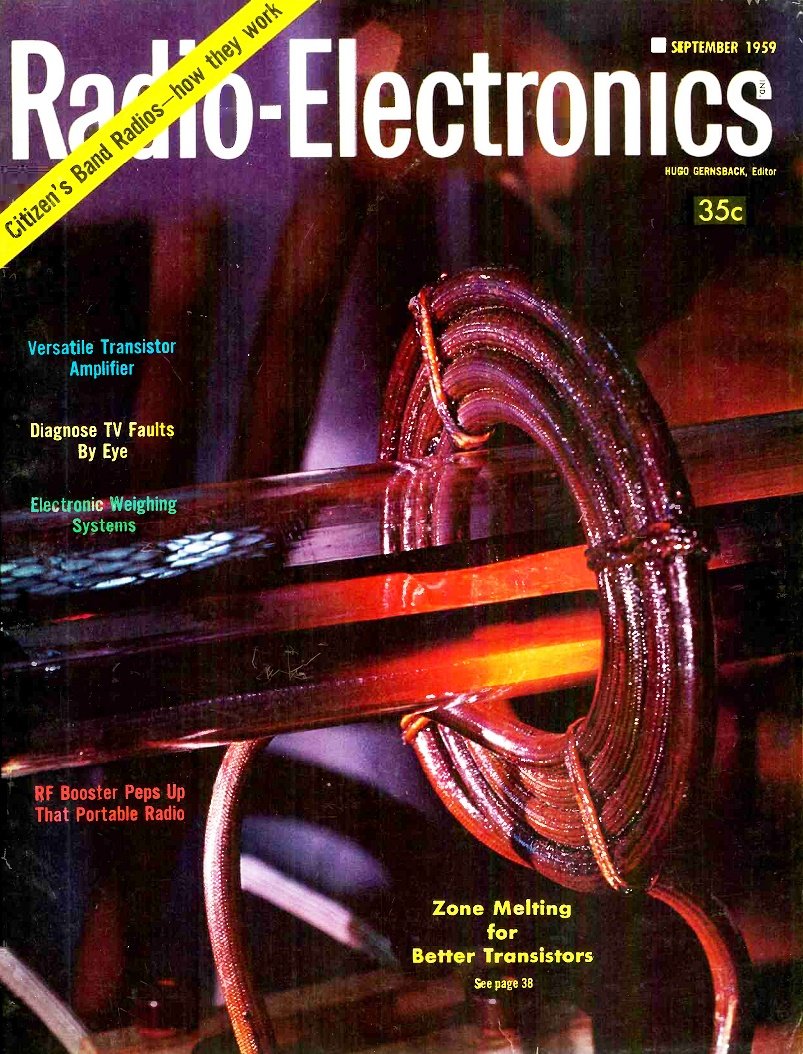
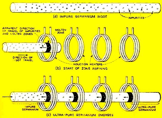
The production of high-performance transistors necessitated new methods to achieve extreme purity levels, far beyond standard industrial capabilities. To reach the required purity of one part in ten billion, engineers adopted zone melting, a sophisticated technique pioneered by W. G. Pfann. In this process, radio-frequency heating coils melt a narrow zone of a semiconductor rod, which is then moved along the crystal to sweep impurities to one end. Beyond purification, zone melting allows for the precise, uniform introduction of "dopants" like antimony or indium, which are essential for creating p-type and n-type semiconductor characteristics. By refining these methods through continuous processing and floating-zone techniques, manufacturers significantly lowered production costs while enhancing device quality. This evolution from batch-processing to advanced, controlled crystallization transformed semiconductors from laboratory novelties into the commercially viable foundation of modern electronics, paving the way for the mass production of reliable, high-precision diodes and transistors. 99.99999999% Pure Germanium
How the material is purified. As the ingot (a single crystal of germanium) is moved through the heater rings, the molten zones travel along it, each carrying a fraction of the impurities toward the end. By Eric Leslie Radio-frequency heating and a novel adaption of an old technique combine to give us low-cost transistors. Semiconductors have made some revolutionary changes in communications techniques. They have also given us new meanings for some old phrases. The expression "99.9`íi pure" used to stand for something very close to the idea of perfection. In a world of transistors, diodes and solar cells, it describes gross impurity. Semiconductors have to be about 99.99999999% pure. This represents an impurity of 1 atom in 10,000,000,000, a number equivalent to one individual in five generations of the whole human race. Chemists have long known how to obtain pure samples of any material that can be crystallized. The substance is melted and part of it formed into a crystal or crystals. In crystallizing, it tends to select atoms that build up the crystal lattice in a regular pattern, so impurities are pretty much left in the melted portion. (An example is the formation of ice in salt water. The salt is driven out and the ice is composed of nearly fresh water.) To increase the purity of such crystals, the material is again melted and the larger portion of it recrystallized. This process can be repeated till a practically pure material results. Such pure materials often act in a startlingly different way than common "99.9% pure" substances, which have one alien atom in every thousand. For example, pure water is an excellent insulator. Yet the purest water available in ordinary life is such a good conductor that a water pipe is always considered a near-perfect ground. The germanium, silicon and other materials used in diodes and transistors do contain impurities, it is true, but these must be of the correct substances and be added in rigidly controlled quantities - quantities so small they would not be detected by ordinary "99.95 pure" methods of analysis. Semiconductor purity must also be gained in a way that will keep diode and transistor production costs low, to permit their general use. The process of repeated crystallization and re-melting has had its triumphs in the discovery of new elements, but the cost per gram (or milligram) of any material so made would forbid its use in most commercial applications. The invention of zone melting by W. G. Pfann of the Bell Telephone Laboratories was the step that made transistors commercially practical. In this technique, instead of melting down the crystal, it is left intact, and only a narrow zone of it melted by induction from an rf heating coil, as shown in the cover photograph and the diagram. The zone is moved along the crystal, leaving the material behind it purer than that ahead. The impurities are carried along in the melted area to the end of the crystal. Several zones may be swept along the crystal, one following the other, as shown in the figure. The end of the crystal containing the impurities is then cut off, leaving ultra-pure material. Various methods of moving the melted zones along the material may be used. A common one is to support the crystal in a cradle of graphite and draw it slowly through a number of coils. In some setups, the crystal remains still and the coils move. Either way, the molten zone must be kept narrow enough for skin tension of the substance to keep the molten material in place. Too large a melted area might cause the material to go out of shape, or even drip. Most semiconductor crystals are made in the form of long rods. If the zone has to be kept narrow, these rods can be made with a small diameter, or the material may be cut into thin plates or even made up in the form of tubes. Can Add Impurities, Too Zone melting is used for another purpose in the manufacture of transistor material. Such elements as germanium and silicon are made into p-type or n-type material by adding fantastically small amounts of impurities, usually in the order of 1 part in 100,000,000. This would be roughly equivalent to two persons in the population of the United States. Antimony might be added to germanium for an n -type crystal, indium for a p-type. To "dope" the crystal with the infinitesimal quantity of impurity required and at the same time assure uniform doping, zone melting is again employed. A small amount of antimony is dissolved in the molten zone to produce an n-type crystal. The amount of antimony that solidifies behind the molten zone is in proportion to the amount of antimony in the melted portion. An exceedingly small amount of antimony solidifies out, so the proportion remains practically the same over the whole crystal. This makes it possible to obtain p- and n-type material of uniform characteristics, producing transistors to closer tolerances. More to Come As great an advance as was the invention of zone melting, recent improvements have made even greater purity and lower cost possible. One of these is a continuous process, making for more efficient production than the crystal-by-crystal batch technique. In effect (though not in mechanical arrangement), new molten material is fed in at the center of the crystal, through which melted zones travel continuously in one direction. Pure semiconductor material is harvested at one end of the rod, while impure material is cut off at the other. A floating-zone technique increases the purity even beyond the figures already given, by holding the material in a vertical position while a molten zone is swept through it by a moving coil. The crystal is supported only at the ends, which are cut off afterwards, so it is in contact with no other material. Thus any chance of contamination is reduced. Still other techniques in the laboratory stage, or starting in production, promise us even better and less costly diodes, transistors and solar cells in the future. |
|||||||||||||
 |
|||||||||||||
|
|||||||||||||

|
||||||||||||||||||||||||||||||||||||