|
|
|||||||||
| Software: RF Cascade Workbook | RF Symbols for Office | RF Symbols & Stencils for Visio | Espresso Workbook | ||||||||||
|
|||||||||||||||||||||||||||||||
   |
  |
||||||||||||||||||||||||||||||
|
Please Support RF Cafe by purchasing my ridiculously low-priced products, all of which I created. RF & Electronics Symbols for Visio RF & Electronics Symbols for Office RF & Electronics Stencils for Visio T-Shirts, Mugs, Cups, Ball Caps, Mouse Pads These Are Available for Free |
|||||||||||||||||||||||||||||||

Evolution of an Integrated Circuit
June 1966
Radio-Electronics
|
June 1966 Radio-Electronics  [Table of Contents] [Table of Contents]
Wax nostalgic about and learn from the history of early electronics. See articles from Radio-Electronics, published 1930-1988. All copyrights hereby acknowledged. |
The first time I ever saw a silicon boule was in my semiconductor physics course at the University of Vermont, circa 1989. For some reason that class gave me trouble. I got a B+ grade, but that was after spending an inordinate amount of time with it. Energy level diagrams, doping, and the equations behind them never quite found a good home in my gray matter. Fortunately, the world has not missed my participation in semiconductor development. When this "Evolution of an Integrated Circuit" article appeared in Radio-Electronics magazine in 1966, germanium was still a fairly large player in the semiconductor world. Silicon began to overtake germanium as the primary semiconductor material in the late 1950s and early 1960s. Germanium was the first material used to create transistors in the 1940s, but it had some limitations, such as its high sensitivity to temperature and its low ability to amplify signals. Silicon, on the other hand, had better electrical properties and was more stable, making it a more practical material for creating electronic devices.
Evolution of an Integrated Circuit
Microcircuits are probably the hottest news in electronics this month, especially since they are being introduced as low-cost items available through ordinary distribution channels. This accessibility should speed their use in consumer products and trigger a raft of experimenters' projects. Here is how IC's are manufactured in quantity - the best way to lower their prices.
Photos courtesy Fairchild Semiconductor Div.
|
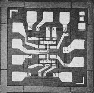
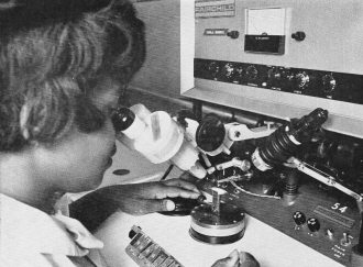
Integrated circuit begins same as other semiconductors: ingot of monocrystalline silicon, "grown" at 1425°C (melt point) in oxygen-free atmosphere. Diffusion steps in IC fabrication: After the first diffusion, following step is to deposit a crystal layer over entire silicon slice. A smooth epitaxial layer is produced this way. Next, isolation diffusions - to keep electronic signals from leaking from one segment to another - are developed in the integrated chip. Other diffusion steps develop a number of transistors, diodes, and resistors. Each element is an integral part of original chip. Still more steps are needed in the diffusion process to complete development of circuit portions. Result is a chip full of active elements. Evaporation apparatus like this is used for depositing interconnects. IC chips are soldered to headers, and thin connecting wires are welded from the bonding points on each integrated-circuit chip to the termination points on the headers. There are different shapes of headers, depending on what style of final packaging is to be used for the integrated microcircuit. Girl above is moving integrated-circuit chip into position for spot-welding the tiny wire leads to the bonding pads at the outer perimeter of the chip - a delicate task that requires of the assembly operator precision, especial care and coordination.
... of the TO-5 variety. The flat package is already finding considerable use in computers, and will undoubtedly be put into consumer products when micro-circuits become available that need the additional connections. As you can see from the preceding photographs, the means for producing cheap microcircuits is already available. It now remains only for the designers to develop new IC's and ways to use them in consumer goods. |
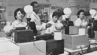
Slices of silicon are coated with a layer of photosensitive material and exposed to ultra-violet light passing through a mask. The patterns which are thus impressed on the silicon substrate form shapes which will then be etched away, leaving behind areas for the many diffusions that are part of the manufacturing process. Mask alignment is simplified by projection-type magnifying viewers shown being used here in IC production. Diffusion is in quartz-tube furnaces. Special gases react with the silicon material to create the desired electrical qualities in the chip. Metallic deposits over and among elements link IC components. Finished chips rest in honeycomb-like carrier awaiting packaging. Powerful microscope for viewing, and special equipment for handling, make final assembly job easier for workers.
The familiar TO-5 transistor can is frequently used as housing for IC's, This packaging is ordinarily merely for convenience in mounting, since a typical integrated circuit chip is tiny in comparison; if there were room for leads, a dozen IC's could be enclosed in a single TO-5 package. The one pictured above is an epoxy-plastic housing placed over a ceramic base. In quantities, integrated circuits in these package types can be sold for considerably less than $5. The "dual-in-line" at right was developed for handling IC's whose lead requirements are greater than can be adapted easily to a package. ... |
Posted April 5, 2023

Copyright: 1996 - 2026 |
About RF Cafe RF Cafe began life in 1996 as "RF Tools" in an AOL screen name web space totaling 2 MB. Its primary purpose was to provide me with ready access to commonly needed formulas and reference material while performing my work as an RF system and circuit design engineer. The World Wide Web (Internet) was largely an unknown entity at the time and bandwidth was a scarce commodity. Dial-up modems blazed along at 14.4 kbps while tying up your telephone line, and a lady's voice announced "You've Got Mail" when a new message arrived... |
Copyright 1996 - 2026 All trademarks, copyrights, patents, and other rights of ownership to images
and text used on the RF Cafe website are hereby acknowledge My Hobby Website: My Daughter's Website: |


