|
November 1963 Radio-Electronics
 [Table of Contents] [Table of Contents]
Wax nostalgic about and learn from the history of early electronics.
See articles from Radio-Electronics,
published 1930-1988. All copyrights hereby acknowledged.
|
Just half a decade
before this "Microelectronics: The Thin Film Approach" article appeared in
Radio-Electronics magazine, Jack Kilby of Texas Instruments and Robert
Noyce of Fairchild Semiconductor had independently announced their creations of
the world's first (and second, but we can't say which is which) monolithic
semiconductor integrated circuit. Specifying "monolithic" is important because
other forms of integrated circuits had been marketed before then - both passive
and active, and both vacuum tube and semiconductor. Monolithic means all the
discrete components were fabricated directly on and within a single
semiconductor substrate. This thin film approach was a hybrid of circuit
printing and component integration that was not a monolithic device, but did
provide many advantages such as very small size, ruggedness, low power
consumption, and high functionality. It was yet another step in the continuing
evolution of microelectronics.
Microelectronics: The Thin Film Approach

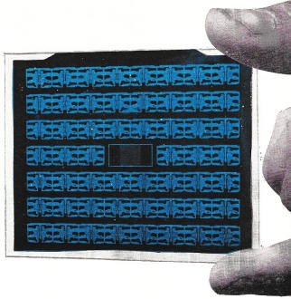
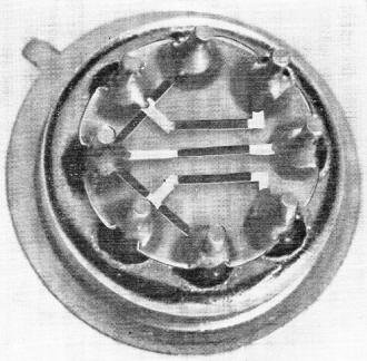
Multi-circuit array of thin-film circuits; below, examples of
finished hybrid circuits - forms of RTL (resistor-transistor logic) flip-flops.
In both cases, thin-film technique has been combined with discrete components.
By C. D. Simmons*
Microelectronics (or microcircuitry) now describes two basic techniques for fabricating
entire circuits-transistors, resistors and capacitors - in a single package no larger
than a postage stamp. How is it done?
In one technique, metallic films are deposited on glass substrates, resulting
in tiny circuit patterns on wafers the size of a contact lens. This gives us thin-film
circuits. The second method produces solid-state semiconductor circuits by diffusing
chemicals into pinhead-size silicon wafers in the same way that transistors are
made.
A third approach now being tried in the laboratories is a combination of these
two basic ones. Thin-film passive components are deposited on the surface of silicon
chips that contain active devices such as transistors.
The thin-film approach is closest to old-time conventional circuitry. Thin-film
circuit elements - separated from the integrated microcircuit and individually packaged
- readily become conventional discrete components, such as the film resistor, for
example.
Not only are the components of thin-film circuitry like conventional ones physically;
circuit design is much the same. We can translate directly from conventional circuit
design to microcircuitry with thin films.
But thin films have at least three striking advantages over conventional circuitry:
miniaturization, performance and reliability. An entire thin-film circuit, such
as a flip-flop, can be packaged in one TO-5 transistor case. Thin-film technique
produces higher quality resistors and capacitors than can be made by semiconductor
methods. (Thin-film resistors have been made with tolerances as close as 0.4%.)
Reliability becomes greater as deposited joints are substituted for soldered or
welded connections. For example, a resistor in a thin-film circuit can be formed
as an integral part of the circuit, rather than with joints between discrete components.

Circuits are getting tinier - being made in one or two steps
... More information about this fascinating frontier of modern electronics.

Fig. 1 - Top and side views of a typical thin-film microcircuit.
Tantalum pentoxide (Ta2O5) is a
good insulator, used both as a dielectric and as a protective skin over resistor
areas.

Fig. 2 - A seven-resistor ladder network. Actual size of
"header" is about 1/4 inch. Resistors are adjusted to 0.04% of design value.

Fig. 3 - Functional circuit of thin-film commutator whose operation
is described in the text. A back bias of +10 volts is applied to A and a and a forward
bias of -10 volts to all other elements to create a path from input 1 to output.
Solid-state microcircuitry will be described in a later article.
To introduce active elements to the thin-film circuit, semiconductors must be
attached to the passive thin film. Active thin-film elements are being worked on
in the laboratory, but have not yet been proved feasible.
Making Thin-Film Microcircuits
Philco uses sputtered tantalum for fabricating resistors, capacitors and conductors
in thin-film microcircuits.
Sputtering is a process based on an electric discharge between two plates in
a gas (generally argon) at low pressure. Ionized gas atoms are accelerated to the
tantalum cathode by a high-voltage field and knock off tantalum atoms. These diffuse
to the glass substrate on the anode. Sputtering wastes little material, and the
deposits adhere excellently. Uniform deposition is possible over large areas (3%
sheet resistivity variation over a 2 1/2 x 3-inch substrate).
Gold is afterward deposited on the tantalum to increase the conductivity of the
conductors and for connections to the package and active elements. A thin layer
of chromium is placed between the tantalum and the gold. This chromium layer acts
as a glue to bond the layers together. Capacitors are formed by anodizing the lower
tantalum layer. This produces an oxide layer (Ta205) on top of the tantalum. This
becomes the dielectric. The capacitor is completed by depositing a gold layer on
top of the oxide. Resistor areas (bare tantalum) are also anodized to form an oxide
layer which acts as a protective skin over the resistor. The active elements - silicon
transistors and diodes - are added in the form of pre-tested chips. Simple photographic
mask changes during the photoengraving make the fabrication process more flexible.
Fig. 1 shows resistor-capacitor construction and an added active element (transistor).
In the Philco process, a vacuum chamber is used only to produce the thin films.
The circuitry is etched externally with high-resolution photolithographic masking.
This eliminates the problems of mechanical masking. The high-resolution photoengraving,
plus the high heat-handling capability of refractory tantalum, permits high density
microcircuitry (more circuitry per unit area). Photoengraving also makes it possible
to design and layout more intricate patterns rapidly at lower setup cost than mechanical
masking. The masking steps proceed as follows: First, the substrate with its initial
tantalum layer is photo-etched and the tantalum removed everywhere except where
a resistor, capacitor or interconnection is to be formed. Then a second photo-mask
is used to expose the remaining tantalum everywhere a resistor or capacitor is to
be formed. This exposed tantalum is then chemically anodized to form an oxide layer.
The chromium-gold multi-layer is placed over the entire substrate and a third set
of photomasks used to remove the gold except where an interconnection, bonding point
or capacitor is wanted.

Fig. 4 - The logic commutator of Fig. 3 ready for insertion in
a circuit. It is encased in a potting compound, and its volume is approximately
a cubic inch.
Hybrid Circuits
Many passive circuits may be produced in a multicircuit array, then cut apart
to add the active elements and assembled into the package (either a multi-lead TO-5
transistor case or a 2-dimensional, 12-lead ceramic-to-metal package). The photos
on the preceding page show a multi circuit array (RTL flip-flop) and assembled units.
A seven-resistor precision ladder network is shown in Fig. 2.
The thin-film diode logic commutator for an aerospace application shown in Figs.
3 and 4 is an example of thin-film circuitry. The matrix consists of 96 silicon
diodes, 24 tantalum film resistors, and associated conductors and interconnections.
The matrix is shown schematically in Fig. 3. The purpose of the finished commutator
(Fig. 4) is to switch 24 different information points or input signals into a single
output channel sequentially. The control diodes, biased by external control circuits,
do the switching. (Input signal swing is limited to ±10v.) For example, if
input 1 is to be monitored, the biasing arrangement would be:
1. Diode bank a receives a back-biasing potential (+10v), while diode banks b
through f are forward biased (-10v). As a result, input signals 5 through 24 are
shunted away out of system through control lines b through f.
2. Control diodes B, C and Dare forward biased (-10v) while diode A is back biased
(+10v). This results in input signals 2, 3 and 4 being shunted out of the system
through B, C and D. Signal 1 then proceeds alone to the output monitor.
* Manager, Microelectronics Div., Lansdale Div., Philco Corp.
|


