|
|
|||||||||
| Software: RF Cascade Workbook | RF Symbols for Office | RF Symbols & Stencils for Visio | Espresso Workbook | ||||||||||
|
|||||||||||||||||||||||||||||||
   |
   |
||||||||||||||||||||||||||||||
|
Please Support RF Cafe by purchasing my ridiculously low-priced products, all of which I created. RF & Electronics Symbols for Visio RF & Electronics Symbols for Office RF & Electronics Stencils for Visio T-Shirts, Mugs, Cups, Ball Caps, Mouse Pads These Are Available for Free |
|||||||||||||||||||||||||||||||
MAT - MOST - MOSFET - UFET - FET: Understanding Solid-State Talk
September 1967 Radio-Electronics

|
September 1967 Radio-Electronics  [Table of Contents] [Table of Contents]
Wax nostalgic about and learn from the history of early electronics. See articles from Radio-Electronics, published 1930-1988. All copyrights hereby acknowledged. |
Abbreviations, acronyms, and initialisms abound in all technical fields, and electronics is no exception. Generally, the coined names are based on the (usually) first letters of words comprising the entity (e.g., metal oxide semiconductor field effect transistor - MOSFET) when the originators are affiliated with private and academic organizations. Government and military groups are famous for twisting and distorting entity names to create descriptive acronyms, like Nanoscale Architectures for Coherent Hyper-Optic Sources (NACHOS), NASA's Space Communications and Navigation (SCaN), and Counter-electronics High-powered Microwave Advanced Missile Project (CHAMP). I just checked in with Wikipedia and found a list of a couple dozen of transistor-related acronyms, which includes MOSFET, DGMOSFET, DGMOS, BJT, SCR, IGBT, JLNT, MNOS, ISFET, BioFET, EnFET, GenFET, DNAFET, CPFET, BeetleFET, DNAFET, finFET, GAAFET, JFET, DEPFET, FREDFET, HIGFET, MODFET, TFET, TQFET, HEMT, HFET, MESFET, NOMFET, GNRFET, VeSFET, CNTFET, OFET, QFET, GFET, VTFET, and others. Determining the meaning and properties of each type is left as an exercise for the reader ;-)
MAT - MOST - MOSFET - UFET - FET: Understanding Solid-State Talk
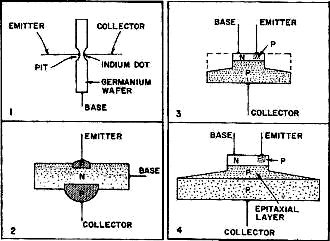
Fig. 1 - First improved junction transistor was the surface-barrier type.
Fig. 2 - With the drift transistor came all increase in upper-frequency limit.
Fig. 3 - To overcome low voltage limit, the mesa transistor was developed.
Fig. 4 - Still higher voltage-handling was built into the epitaxial mesa.
By Rufus P. Turner
Names and abbreviations for the semiconductor family
A quick glance through today's technical literature leaves the impression that the electronics field has as many abbreviations and acronyms as Washington does. And indeed there are quite a few - some bewildering. Consider, for example, MAT, MOST, MOS-FET, FET, UFET, and IGFET!
A great many of these creations are in the family of transistors and related devices. But it was not always so. In the beginning, in the midst of a vacuum-tube population explosion, there was only a transistor-a point-contact thing that resembled a germanium diode with two whiskers instead of one. If the transistor had remained as it was, manufacturers might have varied its characteristics all over the lot but just assigned type numbers like those of tubes - or perhaps even simpler ones,
But along came another kind of transistor, more rugged and stable and easier to make. This junction transistor was dubbed NPN and PNP according to the order in which the negative and positive layers were placed in the semiconductor sandwich. This not only introduced two three-letter symbols, but required that the first transistor also have its own distinguishing initials (PC for point-contact). The letters game was under way.
How Early Terms Grew
Two limitations of early transistors were low input impedance and low operating frequency. The junction transistor didn't improve matters much when it first appeared. Overcoming these shortcomings has spawned many types of transistors, eventually requiring the descriptive acronyms which name them.
First, the surface barrier transistor raised the top frequency capability to 50 MHz and beyond. This new device had a thin base layer and smooth subminiature electrodes, formed through a revolutionary process: Tiny pits were etched in the germanium substrate by electrolysis. Fine jets of metallic (indium) salt solution, carrying direct current, were sprayed against opposite faces of the semiconductor wafer. When the wall between the pit floors was thin enough, the dc polarity was reversed, causing a tiny dot of the metal (Fig. 1) to be plated at the bottom of each pit, forming emitter and collector. The term surface barrier transistor is a good mouthful; so, with typical American zest for abbreviating, we quickly cut that down to SBT. With that step, the family of acronyms grew to PC, NPN, PNP and SBT.
MAT and MADT (SBDT)
Later work showed that operation of the SBT could be improved further by alloying the tiny electrodes to some extent into the semiconductor base. That was done by heating the structure after the indium dots had been deposited deep in the SBT pits. The result was the microalloy transistor (MAT).
Still further work in this SBT family showed that reliability could be increased and parameters controlled more closely by diffusing a base-doping impurity into the semiconductor wafer of the MAT before depositing the electrode dots. The result: the microalloy diffused transistor (MADT). This type has also been called surface barrier diffused transistor (SBDT).
Progressively, the SBT, MAT and MADT (SBDT) offered higher top-frequency operation (important in vhf radio and high-speed computers) than that available with either the PC, NPN or PNP. However, voltage ratings were still low.
The next device to raise the high-frequency limit was the drift transistor. In this alloy-junction unit (Fig. 2), the concentration of impurity in the wafer (base) is graduated, being highest in the region of the emitter. The internal drift field created by this distribution speeds up the transistor's internal currents. Faster action inside the device increases the maximum frequency at which it will operate efficiently.
Hills and Plains
To achieve higher voltage-handling ability to go with improved high-frequency operation, designers evolved a somewhat hill-shaped device which then became immensely popular. The odd appearance results from restricting the junction region to a small swelling atop a much larger semiconductor wafer. The wafer also acts as collector. The post-alloy-diffused transistor (PADT) is one result of this odd conformation.
The starting point of the PADT is the collector - a wafer of P-type semiconductor large enough to handle the desired voltage. First, a thin N layer is diffused into the top of the wafer and becomes the base. Next, a small P region is diffused or alloyed into the thin base and becomes the emitter, and a small pellet of N material is alloyed into the base for contact. Finally, the unneeded part of the wafer is etched away, leaving the emitter and base in the swelling, and the collector occupying most of the remaining wafer.
The SBT, MAT, MADT and P ADT all used a thin base region in a comparatively thick wafer, thus avoiding the fragility of the extremely thin wafer a PNP or NPN would require for high frequencies. But still other higher-frequency units came forth. Fig. 3, for example, shows the cross-section of another transistor in which an extremely thin base layer is deposited in a thick, therefore mechanically rugged, substrate. The starting point is a wafer of P-type semiconductor of the thickness indicated by dashed lines. First, a very thin N layer is diffused into the top of the wafer to form the base. Next, a small P region is alloyed into the N-type base to make the emitter. Finally, most of the wafer structure is etched away, leaving the base and emitter in a little plateau. The Spanish word for hill or table - mesa - names this transistor.
The mesa transistor may be improved (Fig. 4) by forming a thin, high-resistivity layer in the original P material before the N-type base is diffused in. This resistive layer divides the collector into two parts. Because its atoms integrate neatly into the crystalline structure of the collector, the resistive layer is termed epitaxial. This layer permits higher-voltage operation of the epitaxial mesa transistor. What it does is allow heavy doping in the main part of the collector, for low saturation voltage, without reducing the voltage-handling ability of the entire collector.
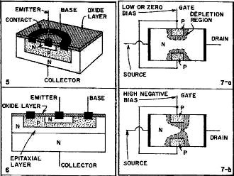
We drop from the hills to the plains when we move from the mesa transistor to one which is processed completely in a flat wafer, hence called planar. The starting point is a wafer of N-type silicon, the bulk of which will become the collector. First, a coat of silicon oxide is formed on the top face. Next, a circular trough is etched out of the oxide; through this "hole," a large P-type base region is diffused and spreads into the wafer (Fig. 5). Then, a concentric disk-shaped area of the oxide is etched away, and an N-type emitter region diffused into the wafer through that bared space. Finally, ring- and disk-shaped contacts are deposited, as shown. The emitter-base and collector-base junctions would be exposed on the top face of the wafer and subject to contamination and short circuit if they were not protected by the oxide layer. The latter is said to passivate the planar transistor.
The advantages of the epitaxial layer in the mesa transistor are available also for the planar. Fig. 6 shows this layer added to the planar structure previously described. The result is the planar epitaxial passivated (PEP) transistor. (Incidentally, we also have PEP diodes.)
Fig. 5 - Planar transistor is so-called because it's shaped like a plain.
Fig. 6 - Planar epitaxial passivated transistor, a further improvement.
Fig. 7a - Basic field-effect transistor uses gate field as control.
Fig. 7b- With high gate field, current flow from source to drain is small.
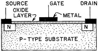
Fig. 8 - The basic insulated-gate FET.
The Field-Effect Family
The devices just described-SBT, MAT, MADT, P ADT, mesa, epitaxial mesa, planar, PEP-improved high-frequency operation of the transistor, and the latter ones in the group also raised operating voltages. None, however, accomplished anything in the direction of increasing input impedance; low input impedance had been a limiting factor in many applications. The first device with high input impedance was the field-effect transistor (FET).
Fig. 7 shows the basic FET. An N-type silicon bar (the channel) has contacts (source and drain) attached to opposite ends, and P regions (gate electrodes) diffused a shallow depth into opposite faces. The source acts like the cathode of a tube, the drain like the plate, and the gate like the control grid.
A depletion region inside the channel surrounds the gate electrodes, as shown in Fig. 7-a. If negative bias voltage applied to the gate is increased, the depletion regions expand toward each other, narrowing the channel and reducing current flow from drain to source. At some high value of bias, the regions meet (Fig. 7-b), closing the channel completely and cutting off the current. Thus, the gate acts like the negative-biased grid of a triode tube. The gate, as a reverse-biased PN junction, is responsible for the FET high input impedance.
The channel may be N-type and the gates negative-biased P-type (as shown in Fig. 7). Conversely, the channel may be P-type material and the gates N-type, in which case positive bias is necessary. Separate acronyms are sometimes used to show which is which: NFET or PFET. The term unipolar field-effect transistor (UFET or UNIFET) also is sometimes used, to denote that the current carriers passing through the channel are of one type-holes or electrons, depending on the type of channel material used. (Conversely, conventional transistors are called bipolar, to indicate that their operation depends upon emission into the semiconductor of carriers of the opposite type. There is no such emitter action in unipolar FET's, since the gates are reverse-biased and serve only to set up a transverse electric field in the channel.) And the term JFET (junction field-effect transistor) may be found in some data.
Higher input impedance than that afforded by the conventional FET - is provided by the device shown in Fig. 8. Separate N regions are diffused (for source and drain electrodes) into a P-type substrate. An oxide layer is formed on the top face of the substrate, and a metallic gate electrode is deposited on top of the oxide. From its configuration, this type of field-effect device is termed metal-oxide semiconductor (MOS), metal-oxide-semiconductor transistor (MOST), or metal-oxide-semiconductor field-effect transistor (MOSFET). It is also sometimes called an insulated-gate field-effect transistor (IGFET) from the fact that the oxide layer insulates the gate electrode from the substrate.
The extremely high input impedance of the MOST results from its almost zero leakage current from the gate, because of the oxide insulation. The dc stability of the MOST is less than that of the FET, possibly also because of the oxide layer, but the MOST is a good rf device.
Other Acronyms
One of the newest solid-state acronyms is RGT-for Resonant Gate Transistor. The heart of each RGT is a tiny solid-gold tuning fork, which makes it possible to tune IC's without bulky coils. A silicon wafer the size of a quarter holds 500 RGTs.
In addition to acronyms and abbreviations which describe the transistors themselves, another one seen on transistor and diode data sheets is JEDEC. This one stands for Joint Electronic Device Engineering Council, and its presence means that the component has been registered by that group and given an identifying number.
Outside of the transistor-diode corner of the electronics world, there are of course many other acronyms - MASER, LASER, RADAR, SONAR, SOFAR, and many more - but that is another story...
Posted October 25, 2023

Copyright: 1996 - 2026 |
About RF Cafe RF Cafe began life in 1996 as "RF Tools" in an AOL screen name web space totaling 2 MB. Its primary purpose was to provide me with ready access to commonly needed formulas and reference material while performing my work as an RF system and circuit design engineer. The World Wide Web (Internet) was largely an unknown entity at the time and bandwidth was a scarce commodity. Dial-up modems blazed along at 14.4 kbps while tying up your telephone line, and a lady's voice announced "You've Got Mail" when a new message arrived... |
Copyright 1996 - 2026 All trademarks, copyrights, patents, and other rights of ownership to images
and text used on the RF Cafe website are hereby acknowledge My Hobby Website: My Daughter's Website: |


