|
June 1968 Radio-Electronics
 [Table of Contents] [Table of Contents]
Wax nostalgic about and learn from the history of early electronics.
See articles from Radio-Electronics,
published 1930-1988. All copyrights hereby acknowledged.
|
Unijunction transistors
(UJT) were relatively new semiconductor devices in 1968 when this article
appeared in Radio-Electronics magazine. Of course for that matter most
semiconductor devices were still relatively new then. Some commercial products
were still being made with vacuum tubes. The "transistor" part of the name is
somewhat of a misnomer due to its physical construction, in that there is no
rectifying PN junction between the two bases, only a single PN junction
(emitter) embedded part-way into the channel between the device's two "base"
connections. There is no collector. The UJT is sometimes referred to as a
double-based diode, although there is no PN junction separating the two base
connections. It usefulness lies primarily in a negative resistance region which
make it a prime candidate for a simple reflex type oscillator. It also is useful
as a triggered switch due to a characteristic where current between the two base
connections increases suddenly at the "peak-point voltage." The UJT operates
somewhat similar to the thyristor, although without a PN junction in the current
path.
20 Unijunction Transistor Applications
 Part 1 of 2 parts-to acquaint you with this
versatile solid-state device Part 1 of 2 parts-to acquaint you with this
versatile solid-state device
By R. M. Marston
All that most electronics amateurs know about the unijunction transistor is that
it is sometimes used as a simple code practice oscillator or as a trigger for SCR's.
Actually, the device has many more uses: It can be used as a very stable wide-range
oscillator, and can be made to generate a whole range of different waveforms. It
can also be made to act as an analog-to-digital converter, as a frequency divider,
as a lamp flasher, as a time-delay unit, or as a number of other useful circuits.

Fig. 1 (left) - Symbol of the unijunction transistor. (center
) - Physical construction of the VJT. (right)- Equivalent circuit of the typical
unijunction transistor.

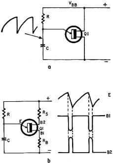
Fig. 2 - (a) A basic relaxation oscillator using the UJT (b)
By adding base resistors, the oscillator is made relatively immune to wide variations
in temperature.

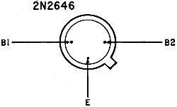
Fig. 3 - Base connections of 2N2646 UJT.

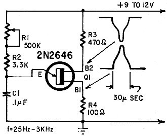
Fig. 4 - Wide-range pulse generator.

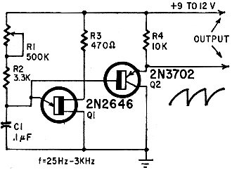
Fig. 5 - Wide-range sawtooth generator.

Fig. 6 - Linear sawtooth (time-base) generator. Frequency range
is 50-600 Hz for a 9-volt supply, and 70-600 Hz for 12.

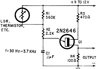
Fig. 7 - Analog/digital converter (resistive); variable resistance
varies the frequency over a range of 30 Hz to 3.7 kHz.

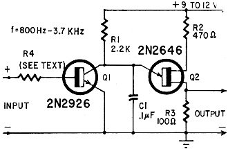
Fig. 8 - Analog/digital converter, shunt type. Variable voltage
applied to input caries frequency from 800 Hz to 3.7 kHz.

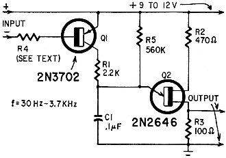
Fig. 9 - Analog/digital converter (voltage), series type. Variable
input voltage swings output from 30 Hz to 3.7 kHz.

Fig. 10 - An improved series type analog/digital converter (voltage
operated).

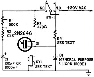
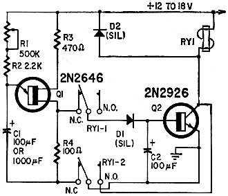
Fig. 11 - Basic relay delay unit. If C1 is 100 μF, delay is adjustable
from about 0.5 to 50 seconds. If C1 is 1000 μF, delay is variable from 3 seconds
to 8 minutes.

Fig. 12 - Another relay delay unit. Time delays are same as specified
for Fig. 11.

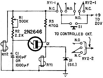
Fig. 13 - Two non-critical relays replace a critical one in this
version of Fig. 11.

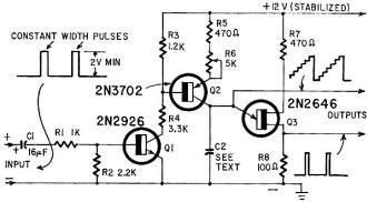
Fig. 14 - This staircase divider/generator can be used to "count"
number of input pulses.
In this article we'll show you what the unijunction transistor is and how it
works. Then we'll introduce you to 20 or so circuits you can build around this amazing
little device.
Basic Theory
The unijunction transistor is a very simple device. Its symbol is shown in Fig.
1-a and resembles the actual construction, as shown in Fig. 1-b. The device is made
of a bar of n-type silicon material with nonrectifying contacts (base 1 and base
2) at both ends, and a third, rectifying, contact (emitter) alloyed into the bar
part way along its length. The third contact forms the only junction within the
unijunction transistor (UJT).
Since base 1 and base 2 are non-rectifying contacts, a simple resistance appears
between these two points. This interbase resistance is that of the silicon bar and
is given the symbol RBB. Normally the value of RBB is between
4000 and 12,000 ohms, depending on the construction of the UJT. It measures the
same in either direction.
In use, base 2 is connected to a positive voltage and base 1 is connected to
ground (or the negative side of the supply). Thus RBB acts as a voltage
divider with a gradient varying from maximum at base 2 to zero at base 1. As the
emitter junction is at some point between base 1 and base 2, some fraction of the
applied voltage also appears between the emitter junction and base 1. This fractional
part of the applied voltage is the most important parameter of the UJT and is called
the intrinsic standoff ratio, or η. The value of η is usually between 0.45
and 0.8.
The equivalent circuit - Fig. 1-c -of the UJT clearly illustrates the above points.
Symbols rB1 and rB2 represent the resistances of the silicon
bar, and diode D1 represents the rectifying junction formed between the emitter
and the bar. When an external voltage (VBB) is applied between base 2
and base 1, a voltage equal to η times VBB appears across rB1.
If a positive input voltage (VE) is now applied between the emitter
and base 1, and is less than η times VBB, diode D1 will be reverse-biased,
and no current will flow from emitter to base 1. Thus, under this condition, the
emitter input appears as a very high impedance. This impedance is that of a reverse-biased
silicon diode, and typically has a value of several megohms.

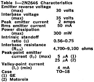
Table 1 - 2N2646 Characteristics
When VE is increased above η times VBB, a point will be
reached where D1 becomes forward-biased and current starts to flow from the emitter
to base 1. This current consists mainly of minority carriers injected into the silicon
bar. These carriers drift to base 1, causing a decrease in the effective resistance
of rB1. This decrease in resistance causes the forward bias of D1 to
increase, thereby causing the current to increase even more, and in turn causing
rB1 to fall even more. A semi-regenerative action takes place, and the
emitter input impedance falls, typically, to about 20 ohms.
Thus, the unijunction transistor acts as a voltage-triggered switch. The precise
point at which triggering occurs is called the peak-point voltage (VP).
It is given by VP = η x VBB + VD, where VD
= forward voltage drop of the emitter diode (usually about 600 mV).
One of the most common applications of the UJT is the relaxation oscillator shown
in Fig. 2-a. Here, when the supply is connected, C charges exponentially toward
VBB via R, but as soon as the capacitor potential reaches VP
the unijunction fires and C discharges rapidly into the emitter. Once C is effectively
discharged, the UJT switches off, C starts to charge up again, and the process is
repeated. A sawtooth waveform is generated between Q1 emitter and ground.
In this circuit, final switchoff actually occurs in each cycle when the capacitor
discharge current falls to what is known as the valley-point current (IV),
generally a value of several milliamps. A minimum current is needed to start the
switch-on action; it is known as the peak-point emitter current (IP)
, typically a value of several microamps.
The frequency of operation of the circuit is given approximately by f = 1/CR,
and is virtually independent of supply line potential. A 10% change in supply voltage
results in a frequency change of less than 1%. The actual value of R can be varied
between a minimum of about 3000 and a maximum of about 500,000 ohms. Hence a very
attractive feature of the circuit is that it can be made to cover a frequency range
greater than 100 to 1, using a single variable resistor.
Frequency stability is very good with changes in temperature, being about 0.04%/°C.
The main cause of this frequency variation is changes in VD with temperature,
these changes being about -2mV/°C. If better frequency stability is required,
it can be obtained either by wiring a couple of diodes in series with base 2, or
by connecting a stabilizing resistor (RS) in the same place.
The interbase resistance of the unijunction increases by about 0.8%/°C, so
the fall in VP (with rising temperature) can be fully counteracted by
the rising voltage on base 2 resulting from the changing potential-divider action
of RS and the interbase resistance. The correct value of RS
is given by
RS = 0.7RBB/η.VBB + (1-η)RB/η
where RB = external load resistor (if any) in series with base 1.
The exact RS value is not, however, of great importance in most applications.
In some circuits, RB is wired between base 1 and ground, as shown
in Fig. 2-b, either to control the discharge time of C or to give a positive output
pulse during the flyback period. A negative-going pulse is also available, if needed,
across RS in the flyback period.
The unijunction transistor used in the circuits below is a 2N2646. Fig. 3 shows
its base connections, while Table I lists its characteristics.
Similar to the oscillator shown previously, the pulse generator of Fig. 4 gives
a large-amplitude, negative-going pulse across R4, and a positive-going pulse across
R3. Both pulses have a voltage amplitude of about half the supply-line value, are
of similar form, and are low impedance. The R4 pulse is suitable for triggering
an SCR.
With the component values shown, the pulse width is constant at about 30 μ
sec over the frequency range 25 to 3000 Hz (adjustable with R1 ). The pulse width
and frequency range can be altered by changing the value of C1. Reducing the value
of C1 by 10 (to 0.01 μF) reduces the pulse width by a factor of 10 (to about
3 μsec) and raises the frequency range by a decade (250 Hz to 30 kHz). C1 may
be from about 100 pF to 1000 μF.
A sawtooth waveform is generated at the emitter, but is at a very high impedance
level and is thus not readily available externally.
Wide-Range Sawtooth Generator
In this circuit (Fig. 5) the saw-tooth waveform from the emitter of Q1 is fed
to emitter follower Q2. Hence the sawtooth appears at the Q2 emitter at an impedance
of about 10,000 ohms. Output coupling may be made, either directly or via a coupling
capacitor, to an external load of 10,000 ohms or greater, without adverse effects
on the waveform or the operating frequency.
Frequency range is about 20 to 3000 Hz with the values shown, so the range is
greater than 100 to 1 via R1. If a smaller range is required, reduce the value of
R1. Operating frequency can be varied from less than one cycle per minute (0.017
Hz) to over 100 kHz by suitable choice of C1.
If an output impedance lower than 10,000 ohms is required, wire a second emitter
follower with an emitter load of 2700 ohms to the emitter of Q2.
Linear Sawtooth (Time-Base) Generator
The sawtooth at the emitter of the basic UJT oscillator is exponential (nonlinear).
In some applications - such as an oscilloscope time-base circuit - a perfectly linear
sawtooth is required. This can be obtained by charging the main timing capacitor
from a constant-current source, as in Fig. 6.
In this circuit, Q1 is wired as an emitter follower with emitter load R4, and
feeds its collector current into the main timing capacitor (C1). The emitter current
of Q1 - and thus the Q1 collector current and C1 charging current-is determined
solely by the setting of R2. It is totally independent of Q1 collector voltage,
C1 charging current is thus constant, and the capacitor therefore charges linearly
up to the striking voltage of the unijunction. At this point Q2 fires and the capacitor
discharges rapidly. Then the timing cycle starts over again.
The signal from Q2's emitter is fed to emitter follower Q3, giving a final linear
sawtooth output at Q3's emitter at an impedance of about 10,000 ohms. This signal
is suitable for feeding to the external time-base input of a scope. In this application,
the flyback pulses from R6 can be taken via a high-voltage blocking capacitor and
used for beam blanking.
This time-base oscillator can be synchronized with an external signal by feeding
the external signal to base 2 of Q2, via C2. This signal, which should have a peak
amplitude of 0.2 to 1 volt, effectively modulates the supply voltage, and thus the
triggering point of Q2. This causes Q2 to fire in sync with the external signal.
C2 should be chosen to have a lower impedance than R5 at the sync signal frequency.
It should also have a working voltage greater than the external voltage from which
the signal is applied.
With the component values shown, the operating frequency can be varied over the
approximate range 50 to 600 Hz using a 9-volt supply, or 70 to 600 Hz using a 12-volt
supply. Operating frequency can be varied from a few cycles per minute to about
100 kHz by suitable choice of C1.
Analog/Digital Converter, Resistive
The circuit of Fig. 7 converts changes in light level, temperature or any other
quantity that can be represented by a resistance, into changes in frequency. The
resistive element (LDR, thermistor, etc.) is wired in parallel with R1, and so controls
the charging time constant of C1, and thus the frequency of operation. A frequency
range of 30 Hz to 3,700 kHz is available, the lower frequency being obtained with
the variable element open circuit.
Output is taken across R4, and consists of a series of pulses. When fed to an
earphone, these can be clearly heard, even at the lowest frequency.
The unit is of particular value in remote reading of such things as temperature,
the output pulses being used to modulate a radio or similar link. At the receiver
end of the link, the digital information can be converted back to analog via a simple
frequency meter circuit.
Analog/Digital Converters, Voltage
These circuits have applications similar to those of the resistance-controlled
circuit. However, their operating frequencies are controlled by voltage or by any
quantities that can be represented by a voltage-photovoltaic cells, thermocouples,
etc.
Figure 8 shows a basic shunt-controlled converter. Q1 shunts the main timing
capacitor (C1 ) and so shunts off some of its charging current and affects the operating
frequency. If zero voltage is fed to Q1's base, Q1 is cut off, and the circuit operates
at maximum frequency (about 3.7 kHz). When a positive voltage is fed to Q1's base,
the transistor is driven on and the operating frequency falls.
A restriction in this circuit is that, as Q1 is driven on, Q1's collector voltage
falls; and when it falls to less than VP, the circuit ceases to operate.
The operating range is thus rather restricted, about 800 Hz minimum in this case.
The value of R4 is chosen, by trial and error, to suit the control voltage in
use. Usually, it will have a value of a few hundred thousand ohms at potentials
up to about 10 volts, and a few megohms at 100 volts.
Figure 9 shows a basic series-controlled converter. Here, the C1 charging current
is controlled almost entirely by Q1. When Q1 is driven hard on (saturated) by a
voltage applied to R4, the charging current is limited by R1, and the circuit operates
at about 3.7 kHz. When zero voltage is applied to R4, Q1 is cut off, and C1 charges
via R5, giving an operating frequency of about 30 Hz. Between these two extremes,
the frequency can be smoothly controlled by the voltage applied to R4 (which controls
the col-lector current of Q1 ). The value of R4 is found by trial and error, as
in the case of Fig. 8.
In the circuits of Figs. 8 and 9, Q1 is cut off until a forward voltage of about
600 mV is applied to its base, so the operating frequency is not affected by voltages
less than this. This difficulty can be overcome by applying a standing bias to Q1
base, as shown in Fig. 10. This modification allows use of input voltages right
down to zero, or even reverse voltages.
Relay Time-Delay Circuits
These circuits enable time delays ranging approximately from 0.5 second to 8
minutes to be applied to conventional relays. That is, there is a delay from the
moment at which the supply is connected to the moment at which the relay switches
on. In Fig. 11, one set of normally closed relay contacts is wired in series with
the positive supply line. Hence, power-supply current is fed to the unijunction
circuit via these contacts. After a delay determined by the setting of R1 and the
value of C1, the unijunction fires and drives RYI on. As RYI switches on, the supply
to the UJT is broken by the relay contacts and the positive supply line is connected
to RYI via R4, holding the relay on.
In this circuit, the relay must be a fast-acting low-voltage type with a coil
resistance of less than 150 ohms. The supply-line potential should be at least 4
times the relay operating voltage. Also, the value of R4 should be chosen to keep
the "on" current within limits when the relay is fed from the positive supply line.
One difficulty with the circuit of Fig. 11 is that the relay type must be carefully
selected. This trouble is overcome in the circuit of Fig. 12. Here, the relay is
connected in the collector of Q2, and is normally unactivated. When the UJT fires,
a positive pulse is fed from R4 to the base of Q2 via D1, driving Q2 and RYI on,
and rapidly charging C2. At the end of the pulse, the UJT switches off and D1 is
reverse-biased, so C2 discharges into the base of Q2, holding the relay on for about
100 msec. Thus C2 is used as a pulse expander, and eliminates the need to use fast-acting
relays.
As soon as RYI starts to close, the negative supply (ground) line to the UJT
is broken via the relay contacts, but is still connected to Q2. Once RYI is fully
closed, the supply is connected directly across RY1, holding it on, and cutting
Q2 out of the circuit.
The relay in this circuit may be any type with a coil resistance greater than
about 100 ohms, and with a working voltage of 6 to 18.
In the two relay circuits considered so far, the relays lock on and draw current
indefinitely once they have been triggered. Fig. 13 shows a different arrangement
of the circuit of Fig. 11, in which two relays are used.
This circuit's positive supply is connected via the normally closed contacts
of RYI and the normally open contacts of RY2. The R Y2 contacts are shunted by pushbutton
switch S1. As soon as this button is pressed, the supply is connected to the UJT
and to RY2, which instantly switches on. When RY2 is activated, its contacts close,
keeping the positive supply connected once S1 is released. After the preset time
delay, the UJT fires, driving RY1 on and thus breaking the positive supply line
to both the UJT and RY2, which switches off and thus completely breaks the supply
to the circuit. The output of this circuit can be taken from the spare RY2 contacts.
When fed with a series of constant-width input pulses, the circuit of Fig. 14
produces a linear staircase output waveform that has a repetition frequency equal
to some subdivision of the input frequency. Alternatively, if the input frequency
is not constant, the circuit "counts" the number of input pulses, and gives an output
pulse only after a predetermined number have been counted. Thus, the circuit can
be used as a pulse counter, frequency divider, or step-voltage generator for use
in such applications as transistor curve tracers.
Circuit operation is as follows: In the absence of an input pulse, Q1 is cut
off, and Q2's base is shorted to the positive supply line via R3, so Q2 is cut off
also, and no charging current flows into C2. If a constant-width positive-going
input pulse is now fed to the circuit via C1, Q1 and Q2 will be driven on and C2
will start to charge via the collector of emitter-follower Q2; the charging current
can be con-trolled via R6. C2 charges linearly, as long as Q2 is on, and since Q2
is on only for the fixed duration of the input pulse, the C2 voltage will increase
by a fixed amount every time a pulse is applied to it.
In the absence of the pulse, there is no discharge path for C2, so the charge
voltage stays on C2. The next pulse again increases the C2 charge by a fixed amount,
until, after a predetermined number of pulses, C2 voltage reaches the trigger potential
of Q3, and the UJT fires, discharging C2 and restarting the counting cycle.
If the input pulses are applied at a constant repetition frequency, the signal
across C2 will be a linear staircase waveform, and an output pulse will be available
across R8 every time the UJT fires. If the input frequency is not constant, the
staircase will be nonlinear, but the R8 pulse will appear after a predetermined
number of input pulses have been applied. Stable count or division ratios from 1
up to about 20 can be obtained.
Finding Division Ratio
Important: this circuit must be fed with constant-width input pulses if stable
operation is to be obtained. Also, the width of the pulses must be small relative
to the pulse repetition period. The value of C2 is determined by these considerations,
and is best found by trial and error. Once a value of C2 has been selected, the
division ratio can be varied over a range of about 10 to 1 via R6.
Now you know how the unijunction transistor works, and you've seen the first
11 projects. In the next article we'll show 9 additional applications.
Continued next month
Posted August 5, 2024
|


 Part 1 of 2 parts-to acquaint you with this
versatile solid-state device
