|
May 1961 Electronics World
 Table of Contents
Wax nostalgic about and learn from the history of early electronics. See articles
from
Electronics World, published May 1959
- December 1971. All copyrights hereby acknowledged.
|
My first experience with negative
resistance was when an engineer I worked for at Westinghouse Electric, in Annapolis,
Maryland, used a tunnel diode to design a simple oscillator circuit. The project
we were working on required an absolute minimum number of parts, with everything
implemented using bare die on a custom polyimide substrate printed circuit board.
I did the assembly, wire bonding, and encapsulation, and often initial test. In
this 1961 Electronics World magazine article, Mr.
Rufus Turner does a nice job of briefly covering the history and application of
negative resistance devices; tunnel diodes were not the first of the kind.
See author's "A.C. Negative-Resistance Devices" article in the July 1963
Electronics World.
Negative Resistance - What It Is & How It's Used
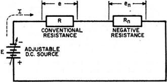
Fig. 1 - Illustration of basic negative resistance principle.
By Rufus P. Turner
Negative-resistance devices have been with us long before the tunnel diode. Here
are descriptions of some of them, along with how and why they operate.
The tunnel diode has turned many minds toward negative resistance for the first
time. Negative resistance is not new, but some electronics people just a few years
ago had not heard of the phenomenon, or had forgotten what they once learned about
it, because they would give a pitched battle on the subject. Always, they challenged,
"How can you make any resistance lower than zero?", which only shows that they thought
in terms of wiping out resistance, not of changing its sign. Zero resistance is
one thing; while negative resistance is something else again.

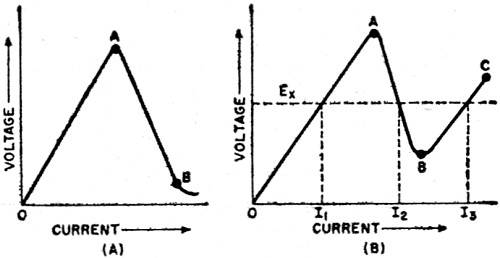
Fig. 2 - Negative-resistance E-I curves.
The concept is easily demonstrated to the dubious, in the following common-sense
terms. Consider a negative resistance (Rn) connected in series with a
conventional (positive) resistance (R) and an adjustable d.c. source (E), as shown
in Fig. 1. The following facts are evident: (1) the same current, I, flows
through all parts of this series circuit and is determined by the voltage E and
the sum of the two resistances (without regard to the negativity of (Rn),
so Ohm's Law is not violated. The interesting point is what happens to the voltage
drops, e and en, produced by this current: whereas e increases with E
and I in the normal manner, en decreases. (Increase I, and en
decreases; decrease I, and en increases.) Thus, the EI curve of this
component must have a negative slope. (2) Irrespective of their magnitudes, however,
e + en =E. So Kirchhoff's Second Law is not violated. (3) Whereas the
conventional resistance consumes power, the negative resistance seems to deliver
power. Actually, the total power supplied by the d.c. source remains the same; it
is only distributed differently between the positive and negative resistances. Thus,
the Law of Conservation of Energy is not violated.
Most negative-resistance devices have a current or voltage region in which their
resistance becomes negative. Outside of this region, the resistance may be positive.
In Fig. 2A, for example, as current through the device is increased, the voltage
drop across the device increases from 0 to A, indicating positive resistance, but
then decreases from A to B as the current is further increased, indicating negative
resistance. In Fig. 2B, there is a negative-resistance region (AB) between
two positive-resistance regions (OA and BC). Thus, at voltage Ex device
current may have anyone three values (I1, I2, or I3).
Another type of negative-resistance device would have the current and voltage axes
swapped. Positive-resistance regions are negative-resistance regions unstable.
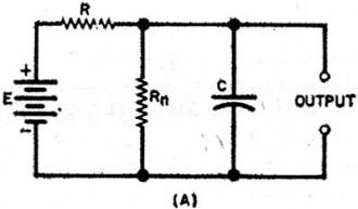
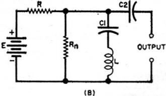

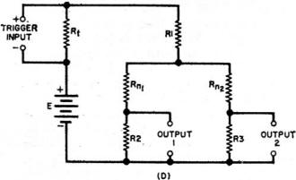
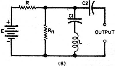
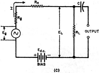
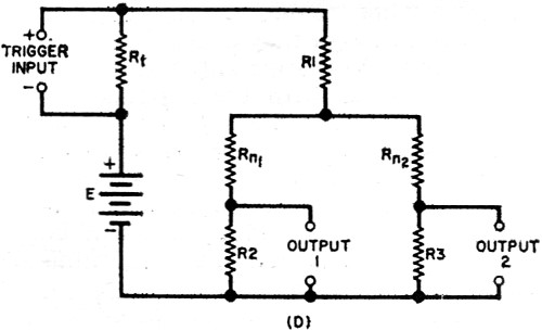
Fig. 3 - Equivalent circuits of negative-resistance devices.
Circuits simulated are (A) relaxation oscillator, (B) sinusoidal oscillator, (C)
amplifier, (D) flip-flop.
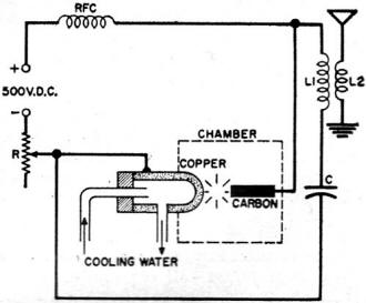
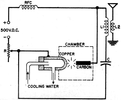
Fig. 4 - The arc-converter transmitter.
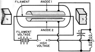
Fig. 5 - The early split-anode magnetron.

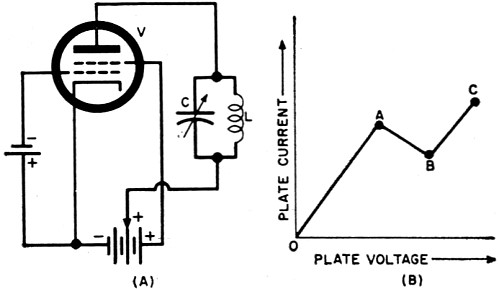
Fig. 6 - Circuit and curve for the dynatron.
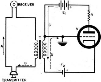
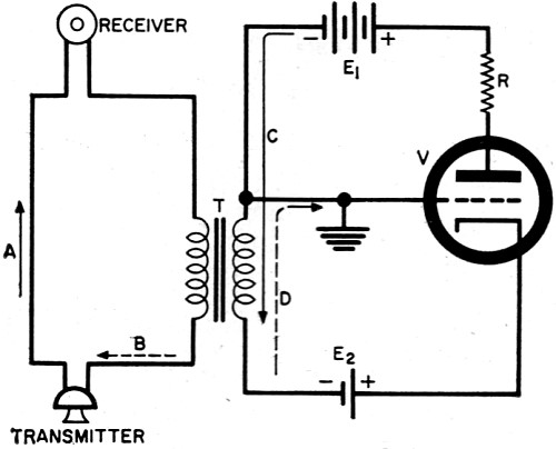
Fig. 7 - Grounded-grid amplifier application.
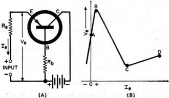
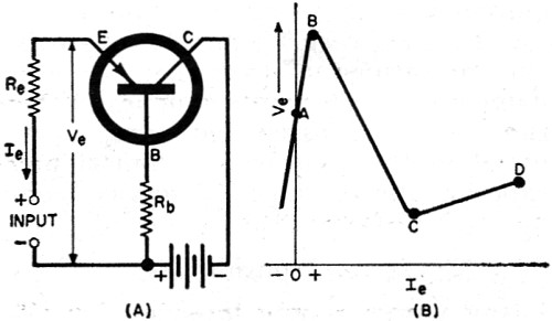
Fig. 8 - Point-contact transistor operation.
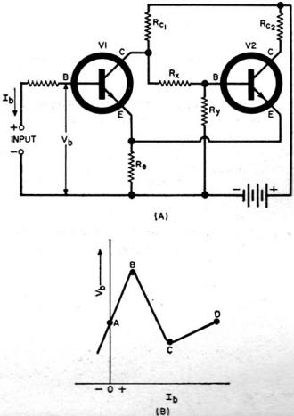
Fig. 9 - The junction-transistor duo circuit.

Fig. 10 - Uni-junction transistor circuit.
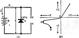
Fig. 11 - Point-contact germanium diode circuit.

Fig. 12 - Circuit showing use of thermistor.
Negative resistance may be put to work for various tasks, such as oscillation,
amplification, frequency conversion, harmonic generation, counting, and switching.
The circuits usually are very simple, since the negative resistor generally is a
2-terminal device. Fig. 3 shows several typical circuits. A rule of thumb is
that when a negative resistance (Rn) is operated from a d.c. supply in
series with a positive resistance (R), shunting Rn with a capacitor (as
in Fig. 3A) produces a relaxation oscillator, and shunting it with an LC tuned
circuit (Fig. 3B) produces a sinusoidal oscillator. Fig. 3C shows one
of many negative-resistance amplifier circuits. Here, the d.c. voltage, Ed.c.,
biases the negative resistor, Rn, into its negative-resistance region,
the a.c. signal is supplied by a generator having internal resistance Rg,
and the output signal is developed across the load resistance, RL If
Rn were not in the circuit, EL would equal EgRL
(Rg + RL). With Rn present, however, operation
is somewhat different. In this case, the gain increases so that the amplifier may
go into oscillation. Here the negative resistance is simulated by the use of positive
or regenerative feedback.
Flip-flop action may be obtained when a negative resistor is operated so as to
provide three-point response, such as shown in Fig. 2B. The device is initially
biased at its lowest EI point (I1 the first stable state in Fig. 2B).
If the voltage then is raised momentarily higher than the value Ex, the
device conduction will flip to the second stable state (I3 in Fig. 2B),
where it will remain until switched back to I1 or until the bias is momentarily
interrupted. Fig. 3D shows a two-legged circuit (with two negative resistors,
Rn1 and Rn2) employing this principle. First, Rn1
in one leg conducts at the low point (I1 in Fig. 2B) and Rn2
in the other leg is at point I3 in Fig. 2B. Momentary increase of
the bias by application of the trigger pulse shifts Rn1 to point I3.
But because of the voltage drop across the common series resistor, R1
both legs cannot be maintained "on" i.e., at conduction point I3) simultaneously.
So Rn2 switches "off" (i.e., to point I1. Thus, alternate
trigger pulses switch the output back and forth between Output 1 and Output 2.
Negative-Resistance Devices
The tunnel diode is a simple, convenient, and practical negative-resistance device
but it is not the first component to provide -R. The answer to the question, "When
were you ever able to buy a negative resistor?" is "For a long time, indeed, but
it was called by other names; negative resistance was not its main function." Devices
which exhibit negative resistance have come forward from the early days of wireless
to the present time, and it seems likely that new ones will be discovered long after
the tunnel diode has become commonplace. The following discussion describes a few
of the most prominent devices other than the tunnel diode. Only d.c.-operated devices
are included.
Arc. In 1900, Dudell discovered oscillation in the d.c. electric arc, and Poulsen
soon put this device to work as a generator of continuous waves which finally actualized
early radiotelephony. (The arc must not be confused with the spark transmitter,
which generates damped waves.)
Fig. 4 shows the basic circuit of an arc transmitter. To increase efficiency,
the arc was operated in a hydrocarbon atmosphere; and, for good heat conduction,
one electrode was made of copper. The applied voltage was from 200 volts to several
kilovolts d.c. and power ratings extended up to 1000 kilowatts. In the 1920's, many
of the high-powered government radio stations were arc-equipped. Long wavelengths
were used. The arc gave way to the more efficient and compact, clean-operating vacuum
tube but it is important historically as an early, high-powered, negative-resistance
device.
Magnetron. The magnetron (first reported in 1921) is a vacuum diode tube in which
negative resistance can be obtained through the action of electrons in a strong
field produced parallel to the tube electrodes by an external permanent magnet.
Fig. 5 shows one type of magnetron. Here, the anode (plate) of the tube is
split into two halves. Electrons tend to pass from the filament or cathode to both
halves of the anode; but actually pass in the greater number (producing high current)
to the half which is at the lower potential. This effect of increasing anode current
by lowering anode voltage corresponds to negative resistance. This type of magnetron
is used up to 1000 mc.; other types at higher microwave frequencies.
Dynatron. Another old-timer (1918) is the dynatron effect in tetrode vacuum tubes.
Fig. 6A shows a typical dynatron oscillator circuit. In this arrangement, the
tube screen is operated at a higher positive voltage than the plate. Secondary emission
from the plate is responsible for the negative-resistance effect. (As the plate
voltage is increased, the velocity at which primary electrons strike the plate and
the number of secondary electrons that accordingly are emitted increase. The secondary
electrons are attracted back to the more positive screen, thereby reducing the plate
current and resulting in the negative slope from A to B in Fig. 6B.)
Grounded-Grid Amplifier. Under certain conditions, a grounded-grid amplifier
provides negative resistance. One such condition occurs in the telephone repeater
amplifier, shown in simplified form in Fig. 7. This amplifier delivers power
to the telephone circuit in which it "rides," instead of absorbing power, hence
qualifies as a negative resistance. Voice currents from the transmitter (microphone)
produce instantaneous currents represented by the dotted arrows, B and D. These
currents, in turn, cause a plate current, represented by the solid arrow C, which
is opposite to D because of 180° phase shift by the tube. This plate current
induces a voltage across the line winding of the transformer, represented by solid
arrow A, which is in series-aiding to the transmitter voltage. This induced voltage,
being in-phase with the speech voltage, aids the latter, causing more current and
power in the receiver. (One of the actions of a negative resistance is, as we have
shown earlier in this article, the delivering of power to the circuit.) When the
amplifier is not operating, the voltage drop across the transformer absorbs power
(positive-resistance action).
Point-Contact Transistor. If positive feedback is introduced in a device which
has a higher-than-1 current gain, the input resistance of the device will be negative
over a portion of the conduction characteristic. The point-contact transistor is
such a device. In Fig. 8A, positive feedback is provided by the external base
resistor, Rb. As the d.c. input (emitter) current is increased, as shown
in Fig. 8B, the emitter voltage (Ve) increases positively to A
and then to B, then negatively from B to C, and positively again from C to D. The
central negative-resistance region (BC), bounded on each side by a positive-resistance
region (AB and CD), gives the type of curve shown earlier in Fig. 2B, which
is valued for flip-flop applications. Viewed from emitter to ground, a point-contact
transistor operated in this manner is a negative resistance.
Direct-Coupled Junction Transistor Duo. The junction transistor has a current
gain of less than 1 when connected regeneratively (common-base circuit), so it cannot
be used directly as a negative resistance in the way that the point-contact transistor
can. However, two junction transistors may be connected in a manner such that a
negative resistance is "seen" at the input terminals of the circuit. In Fig. 9A,
the common emitter resistor, Re is analogous to the common cathode resistor
in a cathode-
coupled tube circuit. Positive feedback voltage is developed across this resistor
by the second transistor, V2. The plot of V1 base voltage
(Vb) vs base current (Ib) has the shape shown in Fig. 9B,
a negative-resistance region appearing between B and C. Viewed from the V1
base to ground, the circuit is a negative resistance when Re has the
proper value to place the operating point of V1 along the negative slope
(BC in Fig. 9B).
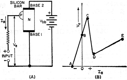
Uni-junction Transistor. This device, also called a double-based diode, consists
of a bar of n-type silicon with an ohmic (non-rectifying) base contact at each end
and a single p-n junction near the top end. Fig. 10A shows a uni-junction circuit.
The junction is biased by the input voltage in such a way that its lower half is
positive with respect to base 1 and acts as an emitter, whereas its upper half is
negative with respect to base 2 and acts as a collector. This simultaneous emitter
and collector action produces a negative-resistance characteristic (region CD in
Fig. 10B).
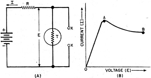
Point-Contact Germanium Diode. The point-contact germanium diode exhibits negative
resistance when biased highly in the reverse direction. Fig. 11A shows the
circuit. As the reverse current is increased from zero (Fig. 11B), the diode
voltage drop increases to A, showing positive resistance. As the current is increased
further, the diode voltage drop then decreases from A to B, revealing negative resistance
which is available at terminals X-X. Unfortunately, the diode is overloaded when
in the negative-resistance condition and is soon damaged by overheating. This has
prevented exploitation of the effect, although the point-contact diode operated
in this manner will oscillate, amplify, and provide bi-stable switching action.
Thermistor. The thermistor, a temperature-sensitive resistor, exhibits negative
resistance over a portion of its EI characteristic, which seems to be dependent
upon internal heating to some extent. The thermistor is not a rectifying device,
therefore it has no polarity; current may be passed through it in either direction.
Fig. 12A shows a thermistor circuit. Fig. 12B shows the response: as the
voltage (E) is increased, the thermistor current (I) increases from zero to point
A, a peak dependent upon internal and ambient temperatures and upon the composition
of the thermistor material. As the voltage is increased further, the current decreases,
as from A to B, revealing negative resistance. The latter is available for use at
terminals X-X.
Because negative resistance in the thermistor depends upon heat effects and since
there can be appreciable thermal inertia in the device, use of the thermistor in
negative-resistance oscillators, amplifiers, and switching circuits is limited to
very low frequencies.
Additional Devices
The devices chosen for review in this article are d.c.-operated, and they qualify
as resistances. In addition to these, there are certain a.c.-operated devices which
can be made to display a negative slope in their conduction characteristics. It
would seem proper, however, to term these negative-impedance devices. In some applications,
these devices are less flexible than their d.c. counterparts because they require
a.c. power supply (either a.f. or r.f.).
Such devices include ferro-resonant elements (ferristors), ferro-electric capacitors,
voltage-sensitive capacitors (silicon capacitors or varactors, and ceramic voltage-sensitive
capacitors), and the several types of magnetic amplifier devices and saturable reactors.
Posted June 27, 2024
(updated from original post
on 6/16/2016)
|