|
December 1974 Popular Electronics
 Table of Contents Table of Contents
Wax nostalgic about and learn from the history of early electronics. See articles
from
Popular Electronics,
published October 1954 - April 1985. All copyrights are hereby acknowledged.
|
Here is the final installment
in the "Basic Digital Electronic Course" series that ran in three issues of
Popular Electronics magazine. The first two parts laid the groundwork with
an introduction to binary, octal, and hexadecimal arithmetic, Boolean logic, AND,
OR and NOT gates, and some truth tables. Armed with those fundamentals, the authors
now dive into flip-flops, encoders and decoders, debouncing circuits for switch
inputs, integrated circuit (IC) types, and interconnect methods to design and build
a simple digital computer with a 7-segment LED display. Don't expect too much from
the computer since it was only three years earlier, in 1971, that Intel introduced
the world's first integrated microprocessor - the 4-bit model
4004 central
processing unit (CPU).
See Part 1,
Part 2,
and Part 3.
Basic Digital Logic Course - Part 3
 By H. Edward Roberts and David Bunnell By H. Edward Roberts and David Bunnell
Part 3: Flip-Flops and How to Build a Very Low Cost computer Terminal
In Parts 1 and 2 of our short course in digital logic, published in October and
November, we discussed number systems, principles of logic, and some basic logic
circuits. This month we will talk about flip-flops and describe the design and construction
of a very low cost terminal (VLCT) for use with computers.
Once you understand the material presented here, you should find that designing
digital circuits - even complex ones - is mostly a matter of common sense and familiarity
with what each element does.
Flip-Flops
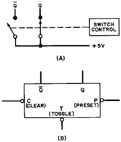
Fig. 1 - Switch analogy (A) and logic (B) of a flip-flop.
The flip-flop is the basic memory circuit used in digital electronics. It has
two stable states that can be simulated by the two-switch analogy shown in Fig.
1A. The switches are arranged in such a way that, if one is closed, the other must
be open, with control circuits determining the states.
The logic diagram of a toggle flip-flop is shown in Fig. 1B. When a pulse appears
at the toggle, or T, input, the Q and Q
(said "not-Q") outputs will change state. The small circle at the T input indicates
that, to toggle the flip-flop, the input must go from "high" (logic 1) to "low"
(logic 0). The other two inputs are labeled P for preset and C for clear. These
allow the flip-flop to be set to a specified condition no matter what was the previous
condition. For example, if a 0 is applied to the P input, the Q output would be
0. Bear in mind that the two outputs are complementary; that is, if Q is at 0, Q
will be at 1.
Semiconductor manufacturers make at least 50 different types of flip-flops. Do
not be intimidated by this number. The flip-flops are still flip-flops, and all
you need to understand any specific one is its data sheet, which you can obtain
from the manufacturer.
Designing a Computer Terminal
Combining what you now know about flip-flops with what you learned in Parts 1
and 2, you have the knowledge needed for designing a VLCT. In the following pages,
we will design a VLCT that will allow you to convert from octal to binary and back
to octal, decimal, or hexadecimal logic. Not only will the VLCT prove instructive
in terms of digital logic, it will also be invaluable for interfacing with other
digital devices. (In particular, it can be used with the Popular Electronics minicomputer
that will be introduced in the January 1975 issue.)
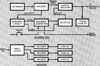
Fig. 2 - Logic flow diagrams of transmitter and receiver.
The VLCT performs seven functions: (1) converts the operator's octal input to
binary format; (2) eliminates any bounce that might be present in the key switches;
(3) loads the binary data into and retrieves it from a register and stores it until
transmission; (4) determines where each piece of data goes in the output register;
(5) transmits a "ready" signal after the third octal number is entered; (6) receives
and stores binary data from the computer; and (7) decodes this computer data in
either octal, decimal, or hexadecimal display format. The overall block diagram
of the terminal shown in Fig. 2 should be consulted whenever any question concerning
functions arises.
The complete logic diagram for the transmitter portion of the terminal is shown
in Fig. 3. The terminal employs transistor-transistor-logic, or TTL, devices - by
far the most widely used logic family. It has the following basic characteristics:
a logic 1 is any potential level between 2.4 and 5 volts, and a logic 0 is any potential
between 0 and 0.4 volt. A detailed discussion of TTL can be found in a number of
books devoted to the subject, but a brief explanation of how a typical TTL NAND
gate works is at the bottom of the page.
Keyboard Encoder
In Fig. 3 the key switches labeled 1 through 7 are grouped together at the upper
left, while the 0 key is located in the center of the diagram. NAND gates NG1, NG2,
and NG3 provide the encoding for key switches 1 through 7, while NG4 detects the
activation of any key.
Before any key switch is depressed, note that NG1, NG2, and NG3 have a 0 output
due to the 1 being applied to each of the four inputs. Note also that NG4 has a
0 output as a result of the 1-level signals applied to its four inputs.
Now, to understand the logic used, assume that key switch 3 has been depressed.
When this happens, one of the inputs of NG1 and NG2 is placed at logic 0 by grounding.
This forces both of these gates to have a logic 1 at their outputs. (A 0 output
of a NAND gate can occur only when all its inputs are a logic 1.) Keyboard output
lines B0, B1, and B2 then have the following conditions:
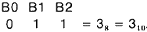
As you can see, the octal input has been converted to a binary code. Note also
that the output of NG4 has gone to a 1, signaling that keyboard activity has occurred.
Depressing key switch 0 causes the output of NG4 to go to 1, indicating that
keyboard activity has occurred. However, this signal will have no effect on NG1,
NG2, or NG3, all of whose outputs remain at 0. If you were to read the binary number
at B0, B1, and B2, it would still be 000 (binary zero). But there would be a signal
from activity gate NG4 to indicate that a switch closure has occurred.
Debounce Circuit
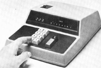
Front view of the computer terminal.

Fig. 3 - Computer schematic diagram.
The problem with many keyboard switches is that they have a mechanical "bounce."
This bounce must be allowed enough time to damp out before attempting to load data
into the output-register flip-flops (FF3 through FF10). This delay is accomplished
in the debounce circuit in which NG5 and NG6 form an RS flip-flop - the simplest
form of flip-flops. To understand its operation, you need to realize that only one
input at a time can be activated by a 0. If a 0 is applied to both inputs at the
same time, the device will not operate as a flip-flop.
 The activity line (output from NG4) goes
to a logic 1 if any key switch is depressed. This signal is fed through inverter
14 to one of NG5's inputs. A zero (0) into NG5 generates a one (1) at the gate's
output, which is then fed to one of NG6's inputs. Assuming that the other input
(pin 5) is also at 1, a 0 will appear at the output of NG6. If both inputs were
allowed to go to 1, the RS flip-flop would remain as set by the previous 0. If a
0 is applied to NG6 while a 1 is applied to NG5, the device will flip, causing a
0 output to be generated at NG5 and a 1 output at NG6. The activity line (output from NG4) goes
to a logic 1 if any key switch is depressed. This signal is fed through inverter
14 to one of NG5's inputs. A zero (0) into NG5 generates a one (1) at the gate's
output, which is then fed to one of NG6's inputs. Assuming that the other input
(pin 5) is also at 1, a 0 will appear at the output of NG6. If both inputs were
allowed to go to 1, the RS flip-flop would remain as set by the previous 0. If a
0 is applied to NG6 while a 1 is applied to NG5, the device will flip, causing a
0 output to be generated at NG5 and a 1 output at NG6.
The mechanical-bounce switch problem occurs whenever a mechanical device is interfaced
with digital electronics. The bounce time of the mechanical switch is very fast
(say, 10 pulses during a 10-ms interval), but it is exceedingly slow from an electronics
viewpoint, since each individual pulse can be detected. A debounce circuit, therefore,
should be included to remove any extraneous pulses.
The debounce circuit employed in the VLCT consists of an RS flip-flop made up
of NG5 and NG6 and a retriggerable monostable multivibrator (sometimes called a
single-shot multivibrator), SS1. The SS1 circuit is basically a form of unstable
flip-flop. When a trigger pulse is applied to it, the multivibrator changes states
only for a period determined by an external-time-delay network, which in this case
consists of C1 and R23 to yield a 10-ms delay. After the delay, SS1 switches back
to its initial state.
Let us trace a signal through the debounce circuit. With a 1 coming from the
output of NG4, the output of 14 is 0. This causes the RS flip-flop to change states,
with the S output going to 1. The logic-1 activity signal from NG4 is also fed to
the B (trigger) input of SS1, causing the multivibrator to go into its unstable
state for 10 ms and apply a 0 to the other input of the RS flip-flop - which is
a violation of the rules for this circuit. But the violation can be disregarded
because SS1 applies this signal for only 10 ms before control reverts back to the
activity input, which sets the S output of the flip-flop to 1. This signal is then
applied to one of the inputs of NG7, while the other input comes from SS1 which,
after 10 ms will apply a 1 to completely enable this gate and generating a 0 at
its output.
The 0 output is inverted by I5 to produce yhe "load" signal for the output register.
It is important to note that the load command did not occur until 10 ms after the
keyswitch was originally closed. This assumes that the switches will not be bouncing
for more than 10 ms. If there were any bouncing after the 10-ms delay, a longer
time constant would be needed at SS1 by selecting appropriate C1 and/or C2 values.
When the key switch is released, SS1 is reset and a "step" pulse is generated'
by NG8 for use by the sequence generator.
Sequence Generator
IC power connections.
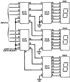
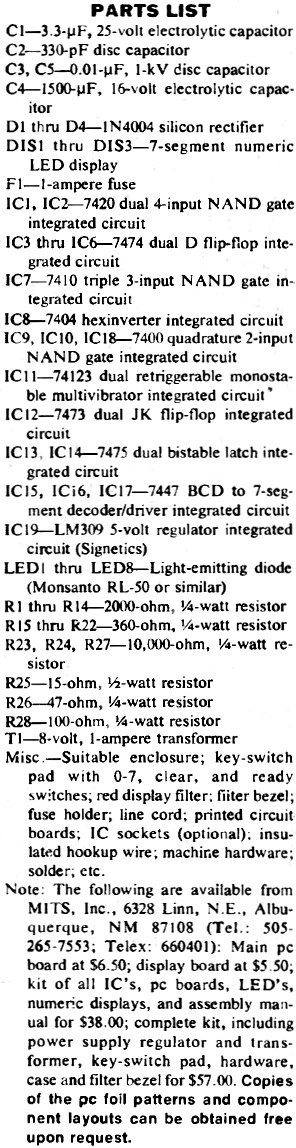
Fig. 4 - Complete logic of the receiver with 7-segment readouts.
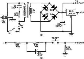
Fig. 5 - Schematic of power supply (A) and "ready" circuits to
be used when terminal feeds a computer (B).
To load eight bits of data into the output register with an octal keyboard, three
switches must be operated because each key depression generates only two or three
bits. For example, assume you want to load the octal number 365 into the output
register. The first step is to load the 3 into the first two bits, the 6 into the
next three bits, and the 5 into the bottom (least-significant) three bits. Note
that the first key depressed can use only two bits. This means that a 3 is the largest
digit allowable on the first key depression. The next two key positions can be any
octal number.
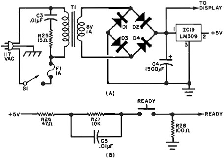
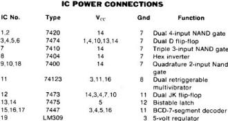
IC Power Connections
The sequence generator consists of FF1, FF2, NG9 through NG14, and SS2. Let us
assume that at the beginning of the cycle FF1 and FF2 are both cleared so that the
Q output of each is 0 and the Q output is 1. Under these conditions, NG11 has a
1 at two of its three inputs. Now, when a load pulse occurs, caused by a key switch
depression, the third input goes to 1 and the output of NG11 goes to 0. After inversion
by NG15, a clock pulse is applied to FF9 and FF10 to cause the data on B0 and B1
to be loaded into FF9 and FF10.
When the key switch is released, a "step" pulse is generated at NG8 and is fed
to the C (clock) input of FF1, causing this flip-flop's Q output to go from 0 to
1; FF2 will be unaffected because the change is positive-going. When the next key
switch is depressed, NG10 will be the gate selected. This will load FF6, FF7, and
FF8 with data from the keyboard. When the switch is released, the step pulse will
again cause FF1 to change states. But this time, the change will be from 1 to 0
at the Q output.
The Q output of FF1 is now 0 and the Q output of FF2 is 1. This selects NG9,
which will load FF3, FF4, and FF5 on the next key switch depression.
When the 3 key is released, the step pulse will again cause the FF1/FF2 counter
to step, resulting in a 1 on both Q outputs. This is detected by NG12 and causes
SS2 to be triggered for 1 μs. Then SS2 clears FF1 and FF2 and transmits a "data-ready"
signal to the computer or other digital devices connected to the output. The CLEAR
button can be used to reset the counter in the event an error was made during entry.
Output Register
The output register consists of FF3 through FF10. These eight flip-flops store
data until the three key entry sequences are completed. They are called data flip-flops,
or D flip-flops. Their function is to load the bit present at the D input whenever
the C (clock) line goes to 1. This data then appears at the Q outputs. The flip-flops
ignore anything on the D inputs unless the clock pulse is present.
The output display consists of light-emitting diodes LED1 through LED8. The LED's
glow whenever their respective data lines are at logic-1. This provides a binary
readout. It is these data lines that are coupled to the external computer or other
digital device.
Receiver
Shown in Fig. 4 is the receiver portion of the system, consisting of latches
IC13 and IC14 (each with four D flip-flops for a total of eight flip-flops); IC15,
IC16, and IC17 4-bit binary to 7-segment decoders; and DIS1, DIS2, and DIS3 7-segment
display readouts.
Assume that the transmitter drives the receiver directly (receiver inputs directly
connected to transmitter outputs). Each time the transmitter receives three key
switch operations during number entry, it transmits a "data-ready" signal to the
receiver. This signal is coupled to the LOAD inputs of quadrature latches IC13 and
IC14 and causes the eight input signals to be read into the two latches and stored.
The outputs of the latches are connected to the 7-segment decoders, each of which
consists of approximately 80 gates arranged to convert a 4-line binary signal into
a 7-segment drive signal for a numeric readout on the displays.
Since the system under discussion is octal-based, one of the inputs of each decoder
is not used. Therefore, each readout displays only the digits 0 through 7. If desired,
the fourth input can be used, resulting in a full decimal and hexadecimal format.
Power Supply

"Now, what do they mean by female connection?"
Shown in Fig. 5 is the power supply for the VLCT. The dc voltage from Ti and
the bridge rectifier consisting of D1 through D4 is applied to 5-volt regulator
IC19. (The +5-volt and ground lines go to the IC's as shown in the table.) The regulator
is current and temperature protected. Capacitor C4 filters the output of the bridge.
The VLCT requires about 500 mA of regulated current for the logic elements and
about 150 mA of unregulated current for the LED displays, both at 5 volts dc.
Construction
The VLCT is assembled on two double-sided printed circuit boards, too large to
be published. The actual-size foil patterns and component layouts can be obtained
by writing to the supplier noted in the Parts List. Carefully install the components
on the boards exactly as shown in the component-placement diagrams. Pay particular
attention to the polarities of the electrolytic capacitors, LED's, and rectifiers
and the orientations and indexing of the integrated circuits and 7-segment displays.
When soldering the component leads to the pc boards, use a low-power soldering
iron and fine solder. Be particularly careful to avoid solder bridges between closely
spaced foil conductors. Note also that the use of sockets or Molex Soldercons®
for the IC's and 7-segment displays is recommended but not absolutely necessary
to assembly.
It is good practice to handle the IC's as little as possible and to install them
as the last step in construction.
The terminal should be housed in a case that allows the display board to be viewed
easily through some form of window. Each LED (indicators for the output register)
should be identified by digit on the cover plate or lens filter as shown in the
photo.
Power transformer T1 should be mounted on the floor or bottom plate of the case,
while regulator IC19 goes on the rear wall, its case exposed to the outside.
Checkout
The checkout procedure consists of making certain that the transmitter is connected
to the receiver and that power is delivered to both circuits. Once it is verified
that power is properly delivered to the circuits, depress three keys on the transmitter
and note that the displays indicate the proper sequence. This procedure checks all
transmitter and receiver logic.
How TTL Works (NAND example)
 Transistor-transistor logic (TTL) is a positive-logic
system. The circuit of a typical gate, in this case one gate in a 7400 quadrature
NAND IC, is shown below. Transistor-transistor logic (TTL) is a positive-logic
system. The circuit of a typical gate, in this case one gate in a 7400 quadrature
NAND IC, is shown below.
If neither input of the gate is grounded, or both are connected to a positive-voltage
source, the base-collector junction of Q1 is forward biased so that current can
flow through R1 and the B-C junction of Q1 into the base of Q2. Transistor Q2 goes
into saturation, producing a voltage drop across R3. This provides a bias to turn
on Q3 and at the same time the voltage at the collector of Q2 drops.
For Q4 to conduct, its base must be at about 1.8 volts. The values of R2 and
R3 are selected so that, when Q2 is conducting, the voltage drop across R3 is high
enough to turn on Q3. But the voltage at the collector of Q2 is not high enough
to cause Q4 to conduct. The "0" output is then only a junction away from ground
(through Q3). Note that in this state, the output (via Q3 to ground) can sink a
reasonable amount of current-approximately 16 mA. This is why TTL is sometimes referred
to as "current-sinking logic."
If one or both inputs of the gate is grounded, Q1 conducts and its collector
voltage drops to near ground potential, cutting off Q2. Almost no current flows
through Q2's C-E junction, and the base voltage ofQ3 (voltage drop across R3) is
close to zero. Transistor Q3 then forms an open circuit. The collector of Q2 approaches
+5 volts, which causes Q4 to conduct. The output (1) is then a function of R4, the
C-B resistance of Q4, and the forward resistance of D1. The output voltage is then
about 3.5 volts.
In the regular TTL family, about 1.6 mA flows through any input grounding circuit.
In the event grounding is through a resistor, there will be a voltage drop across
the resistor. Because the maximum permissible low-state input voltage is about 0.8
volt, the external resistor cannot have a value in excess of 500 ohms, and any low
input connection must hold the input below 0.8 volt.
In some TTL devices, a protective diode is connected from each input to ground.
If a negative voltage (with respect to ground) greater than 0.6 volt is accidentally
applied to either input, the diodes conduct to protect the gate. The protective
diodes also prevent high-frequency ringing when long connection leads or sharp risetime
pulses are used.
The truth table for a two -input NAND gate is as follows:

The 0's and l's represent "low" or logic 0 and "high" or logic 1 conditions,
respectively. Note that the only time the output of the gate changes state from
its normal 1 output condition to 0 is when both inputs are "enabled" (have a 1 applied
to them simultaneously). If neither input, or only one input, is enabled, the output
of the gate remains at 1.
Posted September 20, 2019
|