|
June 1969 Radio-Electronics
 [Table of Contents] [Table of Contents]
Wax nostalgic about and learn from the history of early electronics.
See articles from Radio-Electronics,
published 1930-1988. All copyrights hereby acknowledged.
|
 The introduction of
field-effect
transistors (FETs) into the electronics world was a major benefit to designers
needing lower power consumption and perhaps more importantly, high input impedances
for active circuits. The two most fundamentally distinct type of FETs are the metal-oxide-semiconductor
field-effect transistor (MOSFET) and the junction field-effect transistor (JFET). Both FET types
are voltage-controlled devices and do not require a bias current (hence the high
input impedance) like a bipolar junction transistor (BJT)
does. Neither FET type has a PN junction. A JFET uses a high resistance semiconductor
channel region between the source and drain with an ohmic contact to the gate, whereas
the MOSFET has a insulative oxide layer between the gate and the channel. Check
out the links to each transistor types for more theoretical detail. I don't have
Part 1 yet, but hope to be able to buy the May 1969 issue soon. The introduction of
field-effect
transistors (FETs) into the electronics world was a major benefit to designers
needing lower power consumption and perhaps more importantly, high input impedances
for active circuits. The two most fundamentally distinct type of FETs are the metal-oxide-semiconductor
field-effect transistor (MOSFET) and the junction field-effect transistor (JFET). Both FET types
are voltage-controlled devices and do not require a bias current (hence the high
input impedance) like a bipolar junction transistor (BJT)
does. Neither FET type has a PN junction. A JFET uses a high resistance semiconductor
channel region between the source and drain with an ohmic contact to the gate, whereas
the MOSFET has a insulative oxide layer between the gate and the channel. Check
out the links to each transistor types for more theoretical detail. I don't have
Part 1 yet, but hope to be able to buy the May 1969 issue soon.
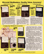
One of the most immediate uses of JFETs was in multimeters to achieve a high
input impedance that imposes very little impact on the circuit being measured due
to the voltage division effect. My first JFET multimeter was a Micronta (Radio Shack)
model 22-208 purchased in 1978. Its $59.95 price in 1978 is equivalent to about
$275 in today's money (per
BBLS Inflation Calculator). Looking at the 1979 Radio Shack catalog
page, compare the input impedance of the el cheapo ($8.95) model 22-027 at 1,000
ohms/volt with the higher end ($49.95) model 22-207 at 100,000 ohms/volt. That means
when a reading of 1 volt is displayed on the scale, the effective internal resistance
of the meter is 1,000 ohms (1 kΩ) and 100,000 ohms (100 kΩ), respectively.
If the circuit being measured (device under test, aka DUT) has an output impedance
of, say, 10,000 ohms (10 kΩ), then the reading is equivalent to what would
be indicated if an infinite impedance meter is used to measure the voltage when
a 1 kΩ or 100 kΩ resistor, respectively, is placed in parallel with the
DUTs 10 kΩ. In the former case, the altered output impedance being measure
then becomes 10 kΩ in parallel with 1 kΩ (abbreviated as 10 kΩ ||
1 kΩ), or 909 Ω (a 90.9% reduction). In the later case, the altered output
impedance being measure then becomes 10 kΩ in parallel with 100 kΩ (10 kΩ
|| 100 kΩ), or 9.09 kΩ (a 9.09% reduction). The 10 MΩ JFET meter
(10 kΩ || 10 MΩ) creates a reduction of only 0.1%. Proof of the preceding
is left as an exercise for the reader.
See part 1 from last month "JFETs: How They Work,
How to Use Them."
JFET's - Part 2
 Build these two useful field-effect transistor
projects - Part 2 Build these two useful field-effect transistor
projects - Part 2
by Ray Clifton
Last month in the first of two articles we looked at the theory and operating
characteristics of a few junction field-effect transistors (JFET's) costing under
$2.50. Now you should be ready to experiment with and build some practical devices
using JFET's.
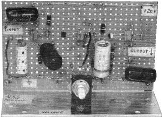
Design a Mike Preamp
You'll need an assortment of 1/2-watt resistors, a few 25-volt electrolytics
and some coupling capacitors. Choose part values around those shown in Figs. 2 and
3. For ease of breadboard experimenting, I recommend a few perforated boards with
push-in terminals. A bias box is needed, since bias is dynamically determined. A
simple arrangement using two 9-volt transistor-radio batteries across a 1-megohrn
linear-taper pot, with a switch to save the batteries, is shown in Fig. 1.
You'll also need a power supply capable of 20 volts and not more than 5 mA-batteries
will do nicely. To test and design the circuit, you will need an audio generator.
(A single frequency of between 400 and 2500 Hz is all you need, and output voltage
can be quite low - 50 mV rms.) An oscilloscope is essential to observe waveforms,
but need not have high-frequency response, since you'll be observing only the frequency
mentioned above. A high-impedance voltmeter (vacuum tube or transistor) is essential,
and a milliammeter is nice, but not essential.
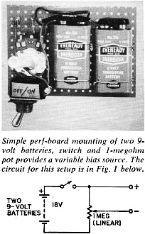
Simple perf-board mounting of two 9-volt batteries, switch and
1-megohm pot provides a variable bias source. The circuit for this setup below.
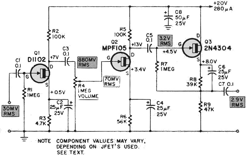
An easy but useful project is a simple preamplifier for a crystal or ceramic
microphone. Fig. 2 shows the circuit, and here's how component values were
selected and the first stage designed.
Assume a microphone output of about 30 mV rms; this calls for a fairly low-level
input JFET. Among those listed in Table I (last month's issue), the D1102 isn't
a bad choice. It has a low gate-to-source cutoff voltage (VP) with reasonable
transadmittance (yfs) and drain-to-source current (IDSS).
The E102 and 2N5033 would also be good choices. (Even better small-signal JFET's
are available, but they cost more than $2.50.)
Like vacuum tubes, most JFET's work well with a gate resistor of 470,000 ohms
or 1 megohm. Remember that the gate circuit is high-impedance and normally doesn't
draw current. Thus, R1 in the input stage is 1 megohm.
The drain-load resistor is also borrowed from vacuum-tube design. The greater
the drain resistor, the higher the voltage gain (AV) of the stage. But
distortion also increases with greater load resistance, and after a certain point
the increase in AV is negligible. For the D1102 at Q1, 100,000 ohms is
a reasonable compromise for R2.
Coupling capacitors C1 and C3 determine frequency response and, for 1-megohm
gate resistors, 0.1 μF provides best low frequency response. You can use 0.05
or even 0.01 with little noticeable loss of low frequencies. If you want only speech-quality
response, use 0.005 μF.
For source resistor R3, temporarily tack-solder in about 4700 ohms, and put the
bias box in series (positive lead to source, negative lead to ground). This allows
you to vary bias until you find the optimum value. Source-bypass capacitor C2 can
be any value from about 10 to 50 μF, at 25 or 50 volts. It's simply a brute-force
audio bypass around the source-bias resistor.
Setting Bias Dynamically
Couple 30 mV of rms audio into C1 and the gate circuit. Set the bias box at 5
volts or more, and tie a power supply to R2, as shown in Fig. 2. The supply
should be 20 volts, ±2 volts. Hang a scope across the output. (You don't
need a load resistor yet, for the output is high-impedance and the scope loads the
circuit.
Note: Be very careful with JFET's. Use heat-sink pliers on the leads when soldering,
and beware of transients, which can zap an FET in a millisecond. Normally a JFET
shows resistance between drain and source, and vice versa. Between gate and either
drain or source, it shows diode action (high resistance in one direction, low in
the other). When zapped, the JFET loses its diode action from gate to channel, and
shows similar resistance in both directions.
With all systems go, decrease source-to-ground bias below 4 volts and watch the
sine wave coming out of the drain. (Use a fairly decent amplifier and speaker to
monitor that sine wave.) Juggle the bias around and observe the scope.
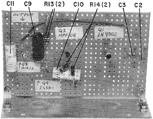
Rear-mounted components for mike preamp.
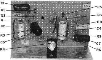
This perfboard arrangement lets you measure voltages and waveforms
easily. Since component values vary, parts such as source-resistor R3 can be tack-soldered
until the correct R4 value is determined.

Fig. 2 - Circuit for a JFET mike (microphone) preamp, which
operates with 30 mV input from crystal or ceramic mikes. Overall voltage gain of
the circuit is about 97.
The JFET's listed in last month's Table I are inexpensive because their parameters
aren't tightly specified. Thus the D1102 you use may have an IDSS of
anywhere from 0.2 to 1.0 mA; the bias you end up using may differ from mine. I found
0.5 volt a safe compromise, and at this bias value my D1102 drew about 100 μA
of drain-source current. By Ohm's law, 5000 ohms is required to cause a drop of
0.5 volt with 100 μA flowing. I chose 4700 ohms as the nearest 10% value (R3).
Drain current then became 115 μA, which had no ill effect on the stage operation.
The second stage - also common-source - can be designed the same as the first,
but you must insert a volume control in the gate circuit or you'll overdrive Q2.
More than about 70 mV rms into the gate circuit causes clipping in the output. The
pot also allows you to increase or decrease gain to compensate for different microphones
and distance between talker and mike. Fig. 2 shows values I obtained for the
Q2 stage with an MPF105, which makes a fairly good medium-level amplifier. Other
suitable devices are the 2N3819, 2N5163, MPF153 and TIS34.
Output stage 03 is a simple source follower to provide fairly low-impedance output,
which makes coupling to following amplifiers less critical than would a high-impedance
drain follower. I used a 2N4304, but a D1201 would also be suitable. Both have a
fairly high VP of 10 volts, which you want in a source-follower output
stage, to handle wide inputs.
The source follower is designed almost like the preceding common-source stages.
The major difference is that load resistor R9 is in the source circuit, rather than
in the drain. This being the case, and since it's desirable to have lower-impedance
output, R9 is made 47,000 ohms instead of 100,000. This provides less voltage gain,
but here you are working with a few volts, so gain is less important. When determining
bias in this circuit, insert the bias box in series with R8 and R9, starting with
about 4700 ohms for source resistor R8. Remember that the gain of a source follower
is never greater than one.
By the way, use decoupling capacitor C8 even if you use a battery supply. It
prevents undesirable inter-stage coupling.
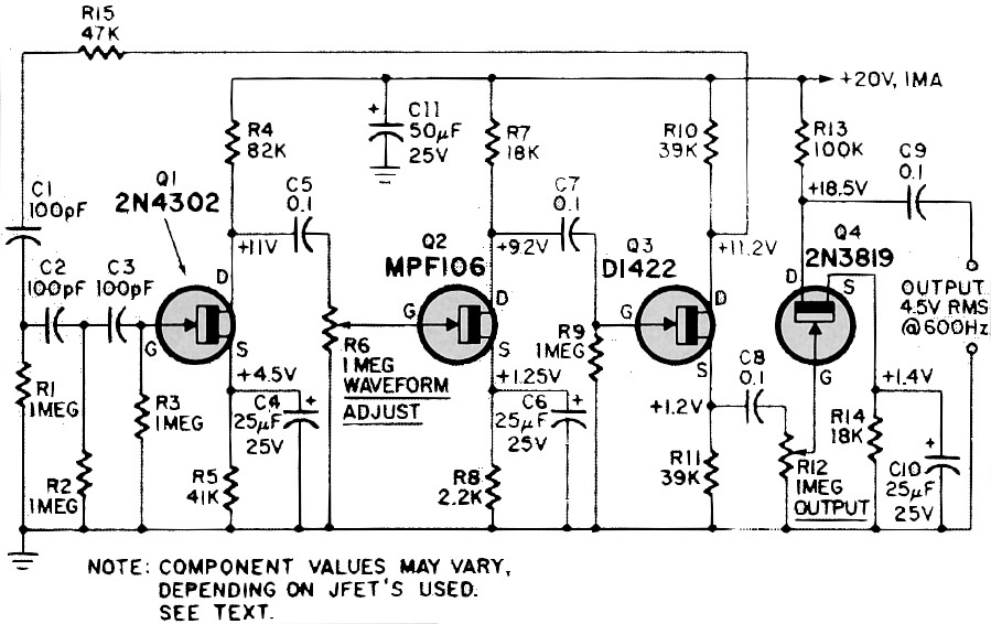
A Simple Audio Oscillator
If you do any experimenting with audio circuits, a small oscillator is handy
to have around. The circuit of Fig. 3 is the basic design for a phase-shift
oscillator using JFET's. Design is fairly straightforward, and is built around the
first stage. If you are willing to spend more money, you can buy a JFET with low
VP and high yfs (the 2N4338, for instance, which costs $4.95)
and build the oscillator with only two stages. (In this case, omit Q2 and Q3, and
tie C1 directly to the drain of Q1.) Unfortunately, none of the devices listed in
Table I have both low VP and high yfs and none will sustain
oscillation from drain to gate. Therefore two more stages are required to provide
sufficient feedback.
Here's how to design the circuit. Build stage Q1 first, temporarily using the
values shown in Fig. 3 for feedback/phase-shift components C1, C2, C3 and R1,
R2 and R3. (Do not connect R15 yet.) You can use 100,000 ohms for drain load R4
(I used 82,000 simply because I had run out of 100K's).
Use the method outlined above to determine bias. From an audio generator, feed
about 1 volt rms into C1. Then provide drain-supply voltage and clamp a bias box
to the source through any value from 1000 to 4700 ohms. Hang a scope and amplifier
on the drain-output circuit and vary the bias until you get the most gain with the
least distortion. Using Ohm's law, determine the value of source resistor R5. I
used 41,000 ohms with the 2N4302. Other choices for this stage are the D1420 and
E102.
The gain of the Q1 stage will be about 30 (too much output) so a pot is needed
between Q1 and Q2. Use a 1-megohm audio-taper pot, to match Q2's input. For Q2 I
used an MPF106, and by trial and error determined that 18,000 ohms was a workable
value for the drain load. Set the bias here as you did before, but don't overdrive
the stage. I found about 35 mV rms from the arm of R6 was about all the stage would
tolerate. Later, this control is used to determine the cleanness of the oscillator
waveform.
The Q3 stage operates as a split-load, providing one output (from the drain)
for feedback and another output (from the source) for output coupling. I used a
D1422, but the 2N4304 and E100 will also work. Try a load resistor of about 47,000
ohms or less to begin with. Then strap in the bias box and determine the source
resistor. If it's less than 47,000 ohms, change R10 to match R11. I ended up with
39,000 ohms in both drain and source circuits. By the way, you should still be using
the external oscillator signal for setting up these stages.
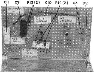
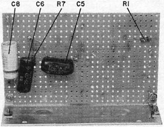
Rear-mounted components for audio oscillator.

To build the JFET audio oscillator, Q1 is mounted and its associated
components temporarily soldered to the push-in terminals. Best bias for Q1 and remaining
stages is determined with the bias box.
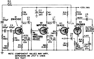
Fig. 3 - This JFET audio oscillator produces clean single-frequency
sinewave. The circuit can be made tunable by changing values of C1-C2-C3 and R1-R2-R3.
Now tie the output of Q3 to RI2 - another 1-megohm audio-taper pot. Remove the
external audio oscillator from Q1 and strap in feedback resistor R15. Try 47,000
ohms to start. You should already have set R6 so it's not overdriving Q2. Hang the
scope across R12 and fire up the circuit. If the output waveform isn't clean, change
R15. (But always turn off the power before you do!) Try less resistance, and if
the waveform gets more distorted, you are going the wrong way. Cut and try until
you find the optimum value. Don't use clip leads to try R15; the stray coupling
will give you a false indication. Tack-solder each value of R15 in place, one by
one.
Once you get the oscillator itself working with a fairly clean waveform, build
Q4. I used a 2N3819 because it has a high VP and hence can accept a fairly
high gate-input signal. The MPF150 and 2N5163 would also be good choices. Transistor
Q4 is simply an isolation stage, and you can assume 100,000 ohms for drain load.
Set the bias as before, being careful not to overdrive the stage with the setting
of R12. I got about 4.5 volts rms out of Q4 with a clean waveform from the oscillator.
Set R6 for purest waveform, and after you build Q4 if you are doubtful of the
oscillator, try another R15. You can vary R12 from zero output up to clipping, and
you should find several volts of output. This output is fairly high-impedance, but
if you prefer low impedance you can make Q4 a source-follower stage. You won't get
as much output, but you'll be able to use a longer output line and match low-impedance
inputs.
Oscillator frequency is determined by R1, R2, R3, C1, C2 and C3, and is about
600 Hz for the values I used. The exact frequency is given by the formula f = 1/10.88
RC, where f is the frequency in hertz, R is the resistance of R1, R2 or R3 (all
equal value) in ohms, and C is the capacitance of C1, C2 or C3 (all equal value)
in farads. Note that this formula holds only if resistors and capacitors are 1%
types. I used 10% types and came up with 600 Hz, rather than the frequency that
was originally computed: 920 Hz.
If you build this circuit on a metal chassis, use a single ground-return bus
insulated from the chassis. Tie the bus to chassis at one point only - the junction
of R1, R2 and R3.
If you want to make the oscillator variable in frequency, sharpen your pencil
and compute the values of R1-R3 and C1-C3 for the frequencies you want. I suggest
using a three-gang capacitor and switching in various resistors. Use straight-line
parts layout and short leads, and put the circuit in a metal box where it won't
be affected by stray capacitance that could alter the frequency.
General Design Notes
The methods outlined above are, of course, very simple. They are meant to show
you how to use JFET's in construction projects. By experimenting with these devices,
you will become familiar with them. Then you can go on to more sophisticated designing.
Because of the spread in JFET parameters, those who design circuits for production
line use must safeguard against device-to-device variation in yfs, IDSS
and VP , They do this by using lots of feedback and sophisticated bias
networks. They also compute drain loads and bias values more exactly, to allow for
temperature and power-supply variations. After you get the feel of JFET's, you may
want to collect some specification sheets on various devices and read up on more
of their characteristics.
Posted August 22, 2023
(updated from original
post on 9/18/2018)
|