|
May 1969 Radio-Electronics
 [Table of Contents] [Table of Contents]
Wax nostalgic about and learn from the history of early electronics.
See articles from Radio-Electronics,
published 1930-1988. All copyrights hereby acknowledged.
|
Last Fall I posted part 2
of this Radio-Electronics article first because I did not yet have the
May issue that contained part 1. So, if you read "JFET's - Put Last Month's Theory to
Work" and have been waiting with bated breath for part 1, you may breathe
easily again; here it is. Author Thomas Haskett enthusiastically introduces readers
to the junction field effect transistors (JFET) as a more natural replacement than
the bipolar junction transistor BJT) for vacuum tubes because of JFET (and other
varieties of the FET) operational parameters being much more those of tubes than
a BJT. Regarding his conversion, Haskett refers to himself as a "die-hard 'fire-bottle'"
man - a term with which I am not familiar. My assumption is that "fire-bottle" is
a slang name for vacuum tubes because of how hot they get, and they glow orange
like a fire in a glass bottle. A Google search on the term turns up a lot of results
for a guitar amplifier overdrive gizmo called the
Fire Bottle, but that is probably not it. Here
is one reference to tubes as "fire bottles" (and
here). If you have a link to a definitive "fire
bottle" definition, please let me know.
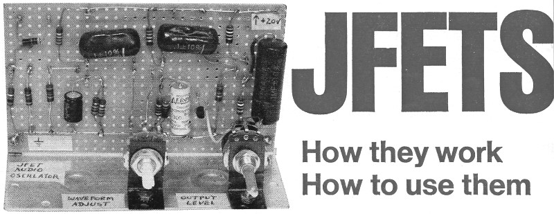
JFETS: How They Work, How to Use Them - Cover Story
 Field-effect transistors have revolutionized
solid-state circuit design. Find out why in this fact-filled series - Part 1 Field-effect transistors have revolutionized
solid-state circuit design. Find out why in this fact-filled series - Part 1
By Thomas R. Haskett
In all electronics, not many devices have been so long awaited or so enthusiastically
welcomed as the Field-Effect Transistor (FET). Many die-hard fire-bottle men (like
me) have been reluctant to use transistors except where they clearly did a better
job than tubes, or where size and portability were major considerations.
Conventional transistors, unlike vacuum tubes, don't provide good input-output
isolation. Their internal feedback causes distortion and requires complex circuits
to deliver fidelity. Further, drift is a problem, and ordinary transistors are highly
susceptible to zapping (burnout).
The FET has overcome many of the disadvantages of the conventional transistor,
and tube lovers who learn about FET's are happy once again. Perhaps you don't realize
that at this moment nearly three dozen different FET's can be had for less than
$2.50 each - many for only a buck. They'll do most of the jobs of vacuum tubes and
many of conventional transistors. In some cases, they'll do better jobs than any
other amplifying devices.
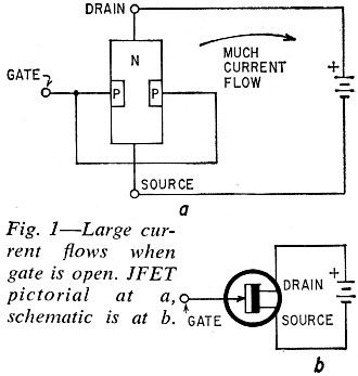
Fig. 1 - Large current flows when gate is open. JFET pictorial
at a, schematic is at b.
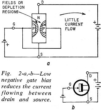
Fig. 2a,-b - Low negative gate bias reduces the current flowing
between drain and source.
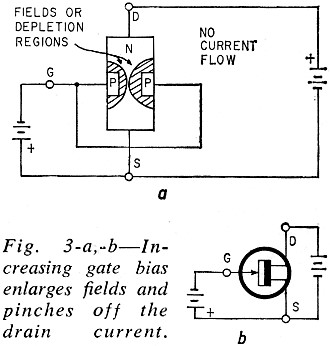
Fig. 3-a,-b - Increasing gate bias enlarges fields and pinches
off the drain current.
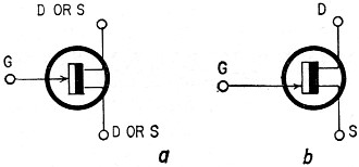
Fig. 4 - JFET's are of two types: a - symmetrical and (b) nonsymmetrical.
Where FET's Have an Edge
The first thing most people seem to learn about the FET is that its high impedance
- like a tube - rather than low impedance - like a conventional transistor. Typical
FET input impedance (Z) is 100 megohms, with an output Z of 100,000 ohms.
Why such high impedance? The FET is a voltage-controlled device - like a tube
- rather than a current-controlled device - like an ordinary transistor. That is,
input voltage controls output current. Because of the FET's high impedance, it can
be used in vacuum-tube circuit designs with little change in components. For one
thing, you don't have to use electrolytics as coupling capacitors, and you can drive
an FET directly from a high-impedance microphone or phono cartridge.
As a DC amplifier, the FET has a zero temperature coefficient. Unlike a tube
or ordinary transistor, it does not drift.
As a general-purpose amplifier, the FET has the high power gain of a vacuum tube
and less noise than either tube or transistor. Of course, it has no filament or
heater, and power requirements are small.
As a vhf mixer, the FET has less noise and cross-modulation than either a tube
or an ordinary transistor. This is due to the FET's nearly perfect square-law transfer
characteristic. Output current varies with the square of the input voltage; hence
the FET produces only second harmonics. Tubes and conventional transistors produce
higher-order harmonics, causing more interference.
Other FET pluses include nearly constant current-output characteristic (flat
drain-current/drain-voltage curves); almost completely unilateral gain function
(nearly perfect input-output isolation), and it can be used as a voltage-controlled
variable resistor (attenuator) when operated at low supply voltages.
One unfortunate disadvantage of today's FET's is that they cannot produce much
output power. The present limit seems to be a few hundred milliwatts. Some manufacturers,
however, are working on power FET's. Such devices would be welcome, and would probably
replace ordinary transistors in output stages.
How the FET Works
There are two basic FET types; this article deals only with the first - the Junction
FET. (The other type will be covered in a later article.) A basic JFET is shown
in Fig. 1-a. It is made up of a bar of n-type semiconductor material with two p-type
junctions diffused in its sides. The p-type junctions are connected together and
called the gate. At one end of the n-type bar is a terminal called the source, which
is connected to the negative pole of the battery. (This terminal is the source of
current.) At the other end of the bar is a terminal called the drain, connected
to the positive pole of the battery. (This terminal drains off current.) Thus current
flows from the negative battery terminal, through the source and the bar (or channel),
out the drain and to the positive battery terminal. The bar acts like a resistor,
for it limits current flow. The schematic symbol for this basic n-channel JFET is
in Fig. 1-b. (It is called an n-channel JFET because the bar, or channel, is made
of n-type material.)
In Fig. 2-a, you see the same hookup as before, except that now another battery
(with lower voltage than the first) has been connected between the gate and source.
Note that the gate is made negative with respect to the source. As shown, little
current flows from source to drain. Why? Because the reverse voltage bias applied
to the gate causes electric fields, or depletion zones, to form around the p-type
gate junctions. These fields oppose and de-crease current flow through the channel,
or bar.
If the gate-to-source voltage is increased enough, as in Fig. 3-a, current flow
from source to drain stops entirely. This level of gate-to-source potential is known
as pinchoff or cutoff voltage. Thus the bar of semiconductor material has become
a variable resistor.
Usually JFET's are made with symmetrical geometry. The symbol for such a device
is shown in Fig. 4-a. Thus it makes no difference which end of the channel you call
the drain or which you call the source - current can flow in either direction. On
the other hand, some manufacturers make nonsymmetrical JFET's. The symbol for such
a device is shown in Fig. 4-b. In this type of JFET, drain and source terminals
are not interchangeable.
Operating Characteristics
A bipolar junction transistor uses both majority and minority current carriers.
In an npn version, for instance, most of the electrons flow from emitter to collector;
they are the majority carriers. Holes flow the other way, and are the minority carriers.
In a pnp bipolar, everything is just the reverse. Bipolars are also called injection
transistors, because of electron-hole injection at the base.
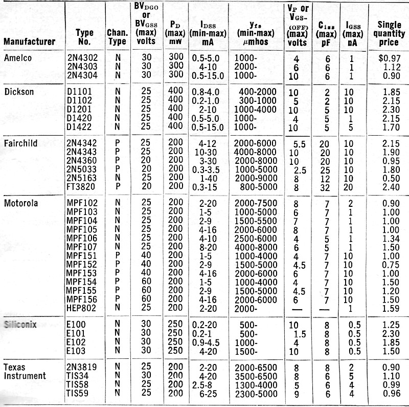
Note: With five exceptions, all devices listed are furnished in epoxy cases.
The five Dickson IFET's are furnished in TO-18 metal cases. In these devices, the
gate is internally connected to the case.
The FET, on the other hand, is a unipolar device. It uses only majority carriers
- electrons in the n-channel version, holes in the p-channel type. (During manufacture,
impurity atoms are mixed into the channel in such density that only one type of
current carriers is available.) And because the gate junction is reverse-biased,
neither holes nor electrons are injected into the channel.
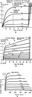
Fig. 5 - Typical curves (a) for JFET, (b) for bipolar transistor,
(c) pentode.
All three types of amplifying devices mentioned above employ some type of input
bias. The gate of a FET is biased by a voltage with respect to the source. The base
of a bipolar transistor is biased by a voltage with respect to the emitter. And
the grid of a vacuum tube is biased by a voltage with respect to the cathode. Note
that a JFET is normally on until reverse-biased at the gate; a bipolar transistor
is normally off until forward-biased at the base, and a vacuum tube is normally
on until reverse-biased at the grid.
Characteristic curves for each of the three devices under discussion appear in
Fig. 5. The JFET drain-voltage/drain-current curves for various values of base bias
are in Fig. 5-b. Bipolar transistor collector-voltage/collector-current curves for
various values of base bias are in Fig. 5-6. Pentode vacuum-tube plate-voltage/plate-current
curves for various values of grid bias are in Fig. 5-c.
Look at Fig. 5-a again and you'll see one important aspect of JFET operation.
As drain-to-source voltage increases from zero, current flows through the channel.
Channel current is approximately proportional to drain-source voltage - up to a
point. This portion of the curve is known as the ohmic region, because the channel
resistance is varied linearly by the current flowing through it. It's also called
the triode region because the curve looks like that of a triode tube. (Near the
bottom of the ohmic region of the curve, channel resistance is several megohms in
a typical JFET.)
But at the knee of the curve, the current has become so great that it sets up
a reverse bias between the gate junctions which acts the same as external gate bias
- it depletes the channel. The curve flattens out because additional increase in
drain-source voltage has little effect on drain current. (The channel resistance
has decreased to about 1000 ohms.)
Since this action resembles pinchoff voltage at the gate, this portion of the
curve is known as the pinchoff region. The channel is saturated with current flow,
so this part of the curve is also known as the saturation region. And since the
curve is flat, like that of a pentode, this area is also called the pentode region.
By operating the JFET in the pinchoff region, with drain-source (Vds)
voltage between about 6 and 12 (referring to Fig. 5-a), small changes in gate voltage
(Vgs) produce large changes in drain current (Id). Thus the
JFET is useful as an amplifier.
Beyond the pinchoff region is the avalanche or breakdown region. It's similar
to the breakdown region in a bipolar transistor. If total device power dissipation
(PD) is not limited to a safe value, the JFET will be destroyed.
Comparison with Other Amplifiers
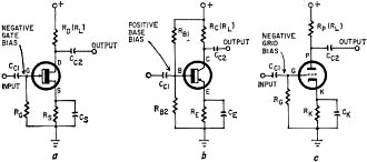
Fig. 6-a - N-channel JFET requires negative gate bias. b-Npn
bipolar transistor requires positive base bias and triode tube (c) needs negative
grid bias.
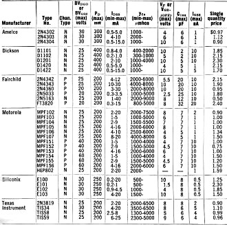
Table I - Low-Cost JFET's
Fig. 7 (above) - Polarities of p-channel JFET (a) and pnp transistor
(b) are opposite from those in Fig. 6.
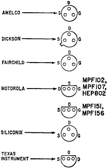
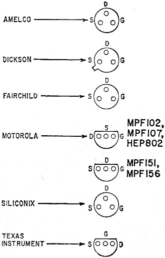
Fig. 8 (top right) - Basing diagrams for the JFET's listed in
Table I, page 25.
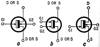
Fig. 9-a, -b (right) - Symbols used for dual-gate symmetrical
JFET's. Non-symmetrical dual-gate JFET uses c.
The similarity between the JFET, the bipolar transistor and the vacuum tube,
when each is used as a simple af amplifier is shown in Fig. 6. In each case, input
is through coupling capacitor CC1 to the FET gate, the bipolar base and
the tube grid.
The FET gate is biased (with respect to the source) by the voltage drop across
RS the source dropping resistor (Fig. 6-a). The tube grid is also biased
by the same method, by the voltage drop across cathode resistor RK (Fig.
6-c). The bipolar transistor is biased by the drop across voltage divider RB1-RB2
between the collector supply and ground (Fig. 6-b). (Some bias also occurs because
of emitter resistor RE, but this resistor is also used for stability.)
In each case a bypass capacitor is used across the lower element - CS
across the FET source resistor; CE across the bipolar emitter resistor,
and CK across the tube cathode resistor. This bypass capacitor allows
its associated resistor to act as a voltage dropper for dc, but not for ac.
Output is taken, in each example, across load resistor RL - which
is called RD for the FET, RC for the bipolar and RP
for the tube. Output is through coupling capacitor CC2.
Now you've seen the similarities of the FET, the bipolar transistor and the vacuum
tube. What about differences? Well, FET's are also made. with p-type channels (see
Fig. 7). Everything here is just the opposite from the n-channel version above.
The channel is p-type material, and the gate junction is n-type material. Drain
voltage is negative and source voltage (ground) is positive. The gate is biased
positive with respect to the source. This is similar to a pnp bipolar transistor,
as Fig. 7-b shows, where the collector is negative, the emitter positive and the
base biased positive with respect to the emitter.
Of course, there is no such thing as a p-channel vacuum tube. If you make the
plate negative with respect to the cathode the tube simply won't conduct.
There are some differences between n- and p-channel FET's. For one thing, the
mobility of electrons is greater than that of holes. Since electrons are the majority
current carriers -which is all that FET's use - in n-channel devices, they are better
than their p-channel counterparts in several respects. The n's have more gain (for
a given input capacitance) than p's. They also have lower on resistance and lower
noise figures. As a matter of fact, n-channel JFET's have the best low-frequency
noise figures of any amplifying device.
All these benefits aren't achieved without a drawback or two. Like all semiconductor
devices, JFET's are manufactured with a rather wide spread of specifications. Table
I lists 35 low-cost JFET's and Table II explains their parameters. Nearly all are
subject to some variation from one device to the next (of the same type number).
For this reason, minimum and! or maximum values are shown. Base terminals for the
listed JFET's are in Fig. 8.
Two parameters aren't shown in Table I because they are somewhat similar for
most of the devices listed. The first is the resistance of the channel: rds(ON).
or drain-to-source on resistance, with gate shorted to source, at 1 kHz. The values
range from about 100 to 3000 ohms, depending on the device, and are useful when
designing a voltage-controlled attenuator. The off resistance is much greater, of
course.
The other parameter not shown in Table I is the noise figure, usually a rating
of spot noise at one frequency. Values range from about 0.1 to 4 dB, but this depends
pretty much on the specified frequency, which can be 1 kHz for audio frequency JFET's
and 100 MHz for vhf devices.
Dual-Gate JFET's
Just as multigrid vacuum tubes are useful for mixing two signals, dual-gate or
tetrode JFET's are used as mixers, converters, and in age service. Schematic symbols
in current use are in Fig. 9; (a) and (b) being symmetrical and (c) nonsymmetrical.
No dual-gate JPET's are listed in Table I because there aren't any which cost less
than $2.50.
There it is, the complete JFET operating theory. Next month we'll put this theory
to practice. We'll show you how to build a JFET preamp for a ceramic microphone
and a simple JFET audio oscillator.
Table II
Important JFET Parameters and What They Mean
BVDGO - Drain-to-gate breakdown
voltage, with source open. A maximum rating, this voltage must not be exceeded or
the device will be permanently damaged (unless power dissipation is limited to a
safe level).
BVGSS - Gate-to-source breakdown
voltage, with drain shorted to source. Also a maximum rating which must not be exceeded
or else permanent damage results (unless power dissipation is held to a safe level).
PD - Total device power dissipation at ambient temperature
of 25°C (77°F). This absolute maximum rating must not be exceeded or the device
will be destroyed.
IDSS - Drain-to-source current,
with gate shorted to source (zero gate voltage). Also called pinchoff or saturation
current. This rating indicates the maximum useful current which can flow through
an output load resistor. Exceeding the maximum IDSS rating causes avalanche
in the device, resulting in permanent damage (unless power dissipation is held to
a safe level).
yfs - Small-signal, common-source,
forward transadmittance (sometimes called gfs-transconductance) at 1
kHz. This is the key dynamic figure of merit for FET's, for it indicates how much
gain is available.
VP or VGS(OFF)
- Gate-to-source pinchoff (or cutoff) voltage. That value of gate bias voltage which
reduces drain-to-source current to a very small amount (usually somewhat greater
than the lass leakage-current value).
Giss -Input (gate-to-source or common-source)
capacitance at 1 MHz. (Also called Cgss and measured with drain shorted
to source.) This rating is particularly important in RF and switching applications.
IGSS - reverse-bias gate-to-source
leakage current, with drain shorted to source. This leakage current, which is usually
low (due to the reverse-biased gate junction) determines input impedance, which
is usually high (several hundred megohms ).
Posted April 30, 2019
|