|
August 1969 Radio-Electronics
 [Table of Contents] [Table of Contents]
Wax nostalgic about and learn from the history of early electronics.
See articles from Radio-Electronics,
published 1930-1988. All copyrights hereby acknowledged.
|
In this final installment of an
"All About IC's" series that appeared in Radio-Electronics magazine in 1969,
author Bob Hibberd discusses how passive components are fabricated in silicon as part
of an integrated circuit. MOS and junction capacitors and diffusion resistors were cutting
edge technology in the day. Although not discussed here, small value inductors could
be made with printed metal on the die. The relatively low frequencies of IC's (a few
MHz at best) meant that most inductive components had to be realized in the form of a
gyrator because there was not enough area available to print a useful
wire inductor. Hibberd also describes the
dicing process,
aka singulation, for breaking individual IC's off the composite wafer. Processes have
changed fairly significantly, but the fundamentals are still the same.
See Part 1,
Part 2,
Part 3,
Part
4.
Making Circuit Components - All About IC's
 by Bob Hibberd by Bob Hibberd
Texas Instruments, Dallas, Texas
How resistors and capacitors are formed - Part 3
Silicon is a resistive material. Its resistivity depends upon the concentration of
current carriers (electrons or holes). To form a resistor in a silicon wafer we diffuse
a suitable impurity into a defined region. The value of this resistor depends upon the
concentration of the impurity, the dimensions of the region at the surface and the depth
of diffusion. Most resistors in IC's are formed at the same time as the p-type transistor
base region. Since carrier concentration and diffusion depth are fixed by the requirements
of the transistor, the width and length of the resistor at the surface determine its
resistance.
The surface concentration of the transistor p-type base region is typically 100 ohms
per square mil. So a resistor stripe 1 mil wide has a resistance of 100 ohms per mil
of length. A stripe 1 mil wide by 10 mils long thus has a resistance of 1000 ohms. By
using several stripes in a series grid form, values up to 20,000 ohms can be made, and
short wider stripes allow values down to 20 ohms. The cross-section of such a diffused
resistor is in Fig. 1.
Fig. 1 - A diffused p-type resistor IC.
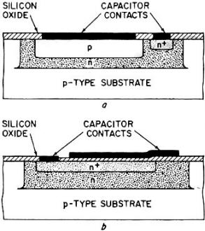
Fig. 2-a, b - Junction and oxide capacitors, respectively.
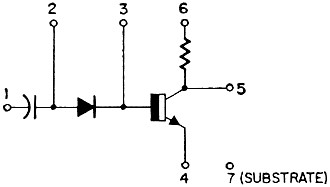
Fig. 3 - Circuit formed in Fig. 4.
When high values of resistance are required, an alternative to increasing stripe length
is to reduce the p-type thickness and effective concentration. This is done by diffusing
an n-type region into it at the same time as the transistor emitter diffusion (dotted
n" area in Fig. 1). This method, however, is harder to control.
For very low values of resistance, down to 1 or 2 ohms, the higher-concentration emitter
diffusion is used to form n-type resistors.
At present, the diffusion process makes it difficult to reproduce diffused resistors
to better than ±10% of the required value. However, the ratio between two resistors
formed side by side can be held within ±1 %. Thus circuit design for IC's tends
to use resistance ratio as a controlling factor rather than the actual resistance value.
This situation will change as improvements in processing allow better reproducibility
of diffusion surface concentration. New techniques are sure to add further improvements.
Integrated Circuit Capacitors
For monolithic IC's two types of capacitors can be prepared - a junction capacitor
or an MOS capacitor. A junction capacitor (Fig. 2-a) uses the capacitance of a reverse-biased
pn junction. It can be formed at the same time as the emitter junction or the collector
junction of the transistor. The value of capacitance per unit area is quite low and the
maximum value used is limited to about 100 picofarads.
Since the capacitance of a pn junction depends upon the reverse voltage, we must arrange
for correct voltage bias in the circuit. Against these limitations, the reverse biased
pn junction has the advantage that it can be formed at the same time as the other elements
with no additional processes.
The structure of a MOS capacitor is in Fig. 2-b. An n+ region is diffused
into the silicon at the same time as the transistor emitter diffusion. It forms the bottom
electrode of the capacitor. A controlled thickness of silicon oxide dielectric is formed
on the surface of this region. The top electrode consists of a layer of metal deposited
at the same time as the interconnection pattern. A somewhat higher value of capacitance
is possible with this method, but is still limited to a few hundred picofarads.
Complete IC Formation
In forming a complete IC, all circuit elements are made simultaneously by the same
sequence of oxidation, selective oxide removal, diffusion and metallization. We can illustrate
this sequence by considering the part of an electronic circuit shown in Fig. 3. For convenience
we assume that the elements are formed in line. In practice, they may be in any disposition.
The steps in the process are in Fig. 4.
The process starts with a slice of p-type silicon, oxidized on the top surface (Fig.
4-a). The first step is the n+ D. U. F. process to give the low series-collector
resistance for the transistor (Fig. 4-b). For each of the diffusion steps, the selective
oxide removal is carried out using the photoresist process.
After the n+ diffusion, the oxide is removed and an n-type epitaxial layer
is grown over the whole surface of the slice (Fig. 4-c). In this n-type layer all the
circuit elements are subsequently formed. The surface is re-oxidized, windows etched
in the oxide and the p-type isolation diffusion carried out to define the regions of
the n-type layer for each element (Fig. 4-d). Next we diffuse the p-type regions for
the transistor base, the diode anode, the resistor and the first capacitor electrode
(Fig. 4-e). Then we diffuse n+ regions for the transistor emitter, the collector
contact, the diode cathode contact and the second capacitor electrode (Fig. 4-f).
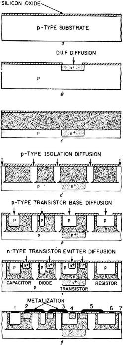
Fig. 4 - Sequence for forming circuit in Fig. 3: in a, a p-type substrate
is oxidized, and in b a n-type diffusion provides collector resistance. Oxide is removed
and a different n layer deposited (c) and re-oxidized. In d, etching and p-type diffusion
defines n-type regions for elements, and in e a p-type diffusion forms more circuit components.
Then an n-type diffusion forms the transistor emitter, diode cathode and capacitor (f).
Step g shows contact and interconnection metallization.
Finally, the metallization pattern is deposited and defined to contact each of the
elements and interconnect them on top of the silicon oxide surface of the slice to form
the complete circuit (Fig. 4-g).
So you don't lose track of size, the overall length taken up by this four-element
assembly is about 35 mils, and the width (into the paper) about 6 mils.
At this stage slice processing is complete. A completed slice is shown in Fig. 5.
The 1.25-inch diameter slice contains approximately 300 complete integrated circuits.
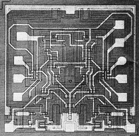
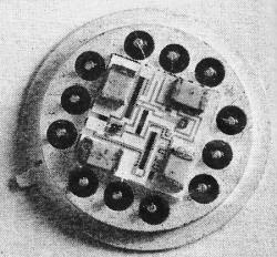
An enlarged view of one circuit is in Fig. 6. On this particular slice, each circuit
is 60 mils square, and contains 8 transistors, 12 diodes, and 12 resistors.
Slice Probe Testing
While still in slices all individual IC's are probe-tested. A typical probe testing
machine has up to 20 pointed probes which can be accurately positioned to make electrical
contact to the terminal contact pads on the IC. On a typical circuit wafer 50 mils square,
there may be 12 terminal pads. After the probes have been aligned to the first circuit,
they must be raised, the slice stepped one circuit along in sequence and the probe head
lowered each time so the probes contact with the pads of each circuit in turn.
Mainly DC tests are performed. A few AC measurements are made, but switching speed
and high frequency tests are limited by the capacitance and inductance of the probe head
and the connections between the probe head and the measuring circuit. Despite these limitations,
it is possible to select good circuits with a probability of about 80%. Any circuits
failing to meet the test standards are automatically marked with an ink spot so that
they can be readily identified and rejected after the slice has been cut into individual
chips.
Individual Circuit Chips
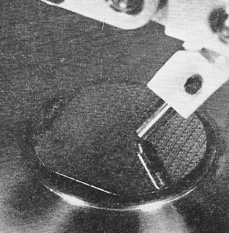
Now the silicon slice is separated into individual IC chips. The most common method
is scribing and breaking, a process similar to glass cutting. Lines are scribed across
the slice between the circuits using a fine diamond point (Fig. 7). Then the slice is
placed on a rubber pad and stressed by running a roller over it. The slice breaks into
the individual chips. The chips are sorted, and rejected units marked with the ink spot
during the probe test are thrown out.
Assembly Processes
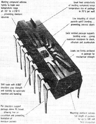
Each IC chip is now assembled into a package, sealed and tested. Two main forms of
packaging are used, a hermetically sealed package called a "flip-pack" because of its
thin rectangular configuration, and a "dual-in-line" plastic molded package. A dual-in-line
is shown in Fig. 8. In each case, the chip must first be mounted into position in the
package. It can be mounted either by soldering down to the base with a suitable metal
alloy or, since electrical contact to the bottom of the chip is not required, a low-melting-point
glass frit can be used to "cement" the chip down.
With the chip firmly mounted in the package, the electrical connections from the circuit
terminal pads on the chip to the package leads are made. The most widely used method
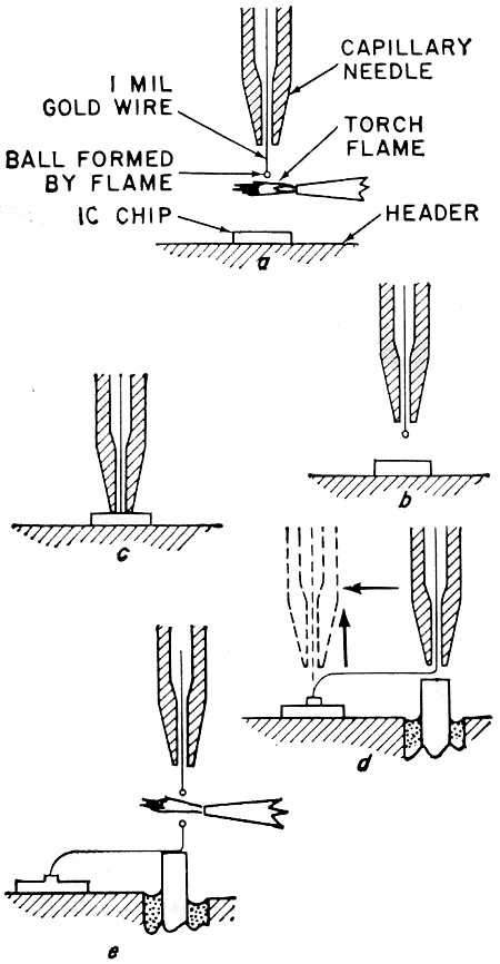
is thermal compression bonding. Gold wire about 1 mil in diameter is used with a process
called "ball-bonding." The gold wire is fed through a capillary needle as in Fig. 9-a.
Then a minute hydrogen flame is passed across the wire, melting it and forming a ball
on the end.
The package with the mounted chip is heated to about 300°C and the capillary lowered
so that the ball on the end of the wire contacts the terminal pad on the chip (Fig. 9-b).
Pressure is applied to flatten the gold ball, and the combination of pressure and temperature
welds the wire to the circuit pad (Fig. 9-c). Then the capillary is raised up the wire,
moved horizontally until it is over the package terminal, and lowered to weld the wire
onto the terminal (Fig. 9-d). After this second weld, the capillary is raised again and
the wire "cut" by passing the flame across the wire. This also forms a new ball on the
end of the wire, ready to repeat the sequence for the next connection (Fig. 9-e).

Fig. 5 - A 1.5-inch silicon slice containing 300 integrated circuits,
each 60 mils.
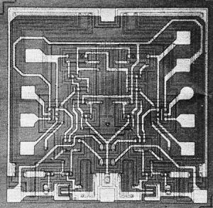
Fig. 6 - View of a typical IC (60 mils sq.).

Fig. 7 - A diamond-point scribe cuts each IC from the slice, similar
to cutting glass.
After all connections have been made, the assembly is ready for finishing. Flat-packs
and TO-5 packages call for welding on a lid to give a hermetic enclosure. With the plastic
unit, the assembly is placed in a mold and the plastic body molded around it. A "leak"
test after sealing checks that the units are completely airtight.
The last step in the manufacture is a series of electrical measurements to determine
whether the performance of the circuit is up to the required standard. The nature of
the final test depends upon the type of circuit, but is a combination of DC and AC measurements
and functional performance of the complete circuit.

Fig. 8 - A dual-in-line IC plastic case.
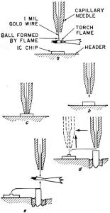
Fig. 9 - Steps a-e show bonding process. Gold wire is heated and melted ball is pressed
to weld wire to pad. Capillary is raised and process repeated for the second (pin connection)
weld point.
Yield Considerations
Many sequential steps go into making an IC. The majority cause some loss. Such yield
losses occur at each of the oxide removal and diffusion steps due to causes such as imperfections
in the original silicon, incomplete cleaning of the slices, uneven photoresist application
and removal, the presence of dust particles and unwanted impurities contaminating the
diffused areas, incomplete control over the etching processes, mechanical breakage of
the slices and so on.
Although the loss at each operation is small, only 1% or 2%, there are so many sequential
operations that the cumulative good yield after scribing the slice into chips and sorting
can be quite low - between 10% and 40% depending on the circuit. After this, additional
good units may be damaged during assembly. And there will be a further loss at final
test due to units not meeting specification. Therefore, the overall yield can be as low
as 5% or perhaps as good as 20%, depending on the type of circuit.
A 5% yield appears extremely low compared to discrete component electronic assembly,
but as 500 circuits are fabricated simultaneously on a slice a 5% overall yield giving
25 good circuits from one slice can be profitable. R-E
Posted September 17, 2018
|