|
Most people today under 30
years old have probably never seen the mechanics or electronics inside their many
personal devices. Everything is so miniaturized and optimized that if something
does go wrong, there is little chance of the owner repairing it. Instead, the phone,
television, stereo, microwave oven, whatever, gets thrown away and a relatively
cheap (compared to paying for a repair) replacement is purchased (or stolen). Besides,
if the item was more than two years old, it was on the verge of obsolescence anyway.
Up until around the early to mid 1980s you had a fair chance of being able to
repair an electronic circuit if trouble arose because at least with commercial products
printed circuit boards (PCBs) were usually 1- or 2-sided and the components still
had leads protruding from the sides of the packages. A $10 Radio Shack soldering
iron and some solder wick was sufficient to remove and replace just about any failed
component. Home brew PCBs could be made to nearly the same quality as commercial
versions using a resist ink pen (basically a Magic Marker) and a dish of ferric
chloride etchant liquid. A drill press helped with making holes for the component
leads, but a hand drill would get the job done. No more, though. If you are resourceful
enough to get your cellphone or camera open without destroying it, you will find
a very neatly laid out, extremely high density PCB with parts so small you might
wonder how they could work at all. Forget servicing the thing with a soldering iron
and a pair of pliers - you will need at least a hot air wand, a magnifier, tweezers,
and, of course, electrostatic discharge (ESD) preventative gear.
In 1949 when this article appeared in Radio & Television News, printed
circuits were just coming onto the scene. Bakelite, steatite, and ceramic substrates
were typically used at the time. Some processes were already using printed resistors
and small-value inductors via silk-screening techniques.
Part 2. A discussion of the techniques and equipment used in making printed circuits
for home-built units (January
1950).
Thanks to Terry W. for providing this article.
Printed Circuits - Part I
This typical group, only a few of the many commercially built
units already produced, is an example of how Centralab's printed circuit audio amplifier
has been received by the industry.
By John T. Frye
A review of printed circuit techniques. To be concluded next month with on article
on how the experimenter can apply, in a simplified form, printed circuits to home
constructed units.
A very loud bang announced to the electronic world early in 1945 that printed
circuits had moved from the experimental to the practical stage, for it was at that
time that the National Bureau of Standards, working closely with the Centralab-Division
of the Globe Union Company, began mass production on the tiny radio proximity fuse
for mortar shells: a fuse incorporating a complex electronic circuit "printed" on
a thin steatite plate 1 3/4" long by 1 1/4" wide!
Since that time, the printed circuit has thrust its tentacles into every portion
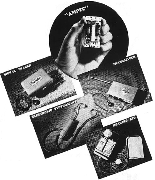
of the electronic field; and it has miraculously shrunk everything it touched. Hearing
aid amplifiers, complete with batteries, that are smaller than a cigarette package;
personal radios that can be cradled in the palm of the hand; radio and television
subassemblies occupying only one-tenth the space needed for conventional assemblies
and requiring one-half as many soldered connections for installation: these are
but a few of the achievements of this new process, and the surface has barely been
scratched. Every day sees new applications of this method by which space is saved,
weight is reduced, assembly is simplified, and cost is cut.
Every electronic worker is certain to come in contact with printed circuits in
increasing number, and it is the purpose of this article to prepare him for that
contact by making him familiar with the various methods and techniques by which
these circuits are produced commercially and then showing him how he can develop
and experiment with his own printed circuits.
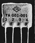
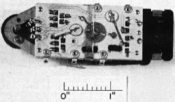
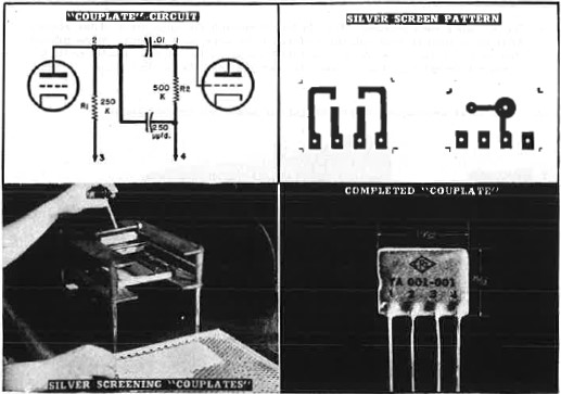
Fig. 1 - The "Couplate" unit. It contains a complete interstage
coupling circuit.
First, it should be clearly understood that the term "printed circuit" covers
any reproduction of an electrical circuit upon an insulating surface by any process.
Essentially it changes a bulky three-dimensional array of electrical parts and conductors
into a compact and very nearly two-dimensional arrangement. An example best shows
how this is done:
Suppose we want to build the complete interstage coupling circuit shown in Fig.
2. First, let us redraw our diagram on a tiny plate of steatite approximately 1"
x 3/4". If. Then let us carefully trace out the heavy lines with a small brush which
we have dipped into a "paint" made by mixing fine particles of silver together with
a liquid binder to hold the particles together and a solvent used to make the mixture
thin enough to brush.
Next, suppose we have several different solutions of finely powdered graphite
or lamp-black, a resin binder, and a solvent. We can experiment with these until
we find just the right combination of mixture, thickness, and length of line needed
to produce resistances equal to R1 and R2; and then we carefully
paint in these resistance lines at the proper points between the silver conducting
lines already drawn. Then we place our little plate in an oven and raise the temperature
to the point where our lines of paint will be "fired" directly to the ceramic base,
adhering to it with a tensile strength of 3000 pounds to the square inch.
Finally we solder tiny ceramic condensers of the proper values across the gaps
representing the condensers, and then we attach flexible leads to our silver paint
at points 1, 2, 3, and 4. The result is a "printed circuit" that will perform exactly
the same as one using conventional components, but our printed sub-assembly will
be no bigger than a postage stamp and require only four soldered connections to
be made by the radio assembly-line operator. A commercial version of just such a
printed circuit is shown in Fig. 1.
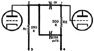
Fig. 2 - Diagram of "Couplate." Finished unit measures 1-1/16
x 13/16 x 3/16 in.
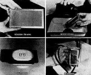
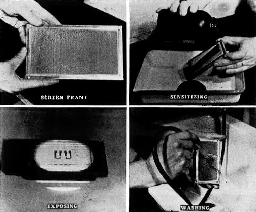
Fig. 3 - These individual operations show the method used
in preparing a silk screen.

Fig. 4 - Silk-screen printing. Paint is forced through the
open mesh of the screen. After the screen is removed. the surface of the base plate
is found to be printed with an exact, sharp-edged, uniformly thick design of the
required conductor circuit. A second stencil can then be used to print the resistors
in their proper location.
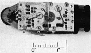
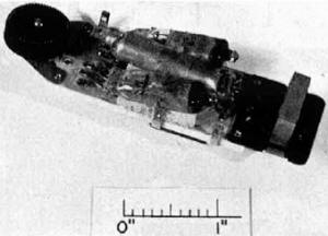
Fig. 5 - Front and rear views of one of the many hearing-aid
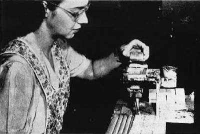
amplifiers that are printed on ceramic plates.
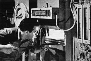
Fig. 6 - A high temperature oven is used for firing a group
of printed circuits. (Note lack of hand and eye protection)
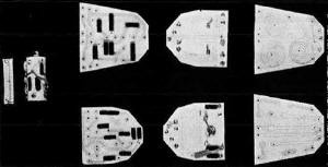
Fig. 7 - Partially completed electronic circuits printed
on steatite plates and cylinders by the silk-screen process. Light lines are silver
conductors and inductors; dark rectangles are resistors; circular disks are ceramic
condensers.
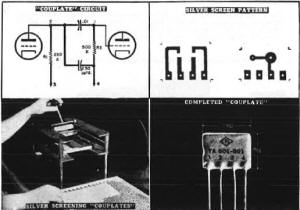
Fig. 8 - Illustrating the evolution of an audio plate-to-grid
coupling circuit.
Such a manual process, while pointing up the difference between printed and conventional
circuits, obviously could not be adapted to mass production. Various stenciling
methods are the answer to producing more uniform circuits at higher speed, and the
silkscreen process is one of the most successful.
In this system, a fine-meshed silk screen is tightly stretched on a wooden frame
and covered with a photosensitive material that becomes insoluble when exposed to
strong ultraviolet light. A photographic-positive mask of the exact shape of the
required conducting circuit is placed on top of the screen, which is then exposed
to the rays from an ultraviolet lamp. Finally, the portions of the film protected
by the mask are washed away in cold water, leaving a stencil of the conductor design
to be printed. All four of these steps are clearly illustrated in Fig. 3.
This finished stencil is held securely against the base plate to be printed;
and the circuits can be printed on practically any insulating material, or even
on conducting material that has been coated with a non-conducting film, such as
lacquer, and a quantity of silver paint is placed at one end of the screen. A neoprene
bar, or "squeegee," is moved across the top surface, forcing the paint ahead of
it and down through the open mesh of the design, as is shown in Fig. 4. When
the screen is removed, the surface of the plate is found to be printed with an exact,
sharp-edged, uniformly-thick design of the required conductor circuit. A second
stencil can be used to print the resistors in their proper places. The paint is
fired to the base exactly as was done before. This process is shown in Fig. 6.
In Fig. 7 are displayed base plates at various stages of completion.
Brushing and stenciling with a silk screen are not the only ways in which the
conducting and resistor paints are applied. For example, a decalcomania, .on which
the circuit is printed on a thin flexible film that can be transferred to the final
surface, is useful in applying the circuits to cylindrical or irregularly-shaped
objects. The film is removed by firing.
Most standard printing processes are also used. As a single example, the required
design can be raised on the face of a rubber stamp, and this stamp can be pressed
first on a pad of conducting ink and then on the surface to be printed. Plating
of this printed design will increase its conductance if necessary. In the same way,
other printing processes such as engraving, lithographing, and intaglio are also
employed.
You old-timers who used to draw your own grid-leaks with a lead pencil were using
a form of printed circuits that still may have possibilities. Pencils having "leads"
of varying degrees of conductivity, or pens filled with conducting inks are being
used experimentally. With such devices an experimental circuit could be drawn and
constructed ready for testing all at one and the same operation!
Condensers can be painted, too, by employing silver disks painted on opposite
sides of the base plate so that the plate material becomes the dielectric. If the
plate is constructed of high-dielectric material, condensers of reasonable capacity
can be obtained by this method; otherwise, miniature thin-disk ceramic condensers
are often employed by soldering them with a low temperature solder directly to a
silvered area on the base.
Printed inductors are also used, especially in the low-inductance values. Spiral
forms are used on flat bases, although the more conventional forms can be used when
the circuit is printed on the tube envelope or a cylindrical base plate as is shown
in Fig. 9. The inductance of a spiral conductor can be increased by covering
it with an insulating layer of lacquer and then painting another spiral right on
top of it and connecting the two in series, painting another spiral on top of that,
etc. The distributed capacity and the Q of the circuit required are the limiting
factors to the usefulness of this method.
Placing a layer of magnetic paint, made of a colloidal suspension of powdered
magnetic material, both beneath and above the spiral conductor, with insulating
layers serving to protect the turns of the inductance from shorting. will also increase
the inductance.
The spraying of conducting films on insulated surfaces is another method of printing
circuits. The same paints can be used in paint spray guns as for the stenciled-screen
process; or molten streams of metal can be sprayed through locating stencils. Guns
are available in which the metal to be sprayed is fed into the gun in the form of
a wire, where it is heated to the melting point by a hydrogen-acetylene or other
flame. Compressed air is used to atomize the molten metal and to drive it on to
the work. This molten material can .be sprayed on wood, Bakelite, plastic, and even
ceramic surfaces.
One popular method employs a plastic base plate. This plate is sandblasted through
a mask so that shallow grooves are cut where the conductors are needed. These grooves
are sprayed full of molten metal, after which the surface can be milled, leaving
conducting lines that are flush with the surface of the plastic base plate.
Still another scheme uses an insulated base plate with a thin evaporated coating
of conducting metal. This is covered with a photosensitive film and exposed to light
through a mask. The film is developed so that the portions exposed to light are
removed, and the remaining portions, outlining the desired circuit, resist an abrasive
spray so that the protected portions beneath remain intact while the rest of the
metallic coating is cut away by the sand blast.
Another method of producing "printed circuits" is by chemical deposition. This
method is not used much on a commercial basis because of the very thin layers deposited
and other technical difficulties, but it consists essentially of depositing a thin
silver coating on a masked surface by the same chemical methods that are used in
silvering mirrors. Increased conductivity can be secured by repeated silvering or
by plating.
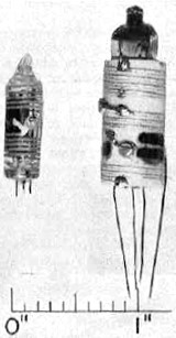
Fig. 9 - Two complete high-frequency transmitters ready
to be connected to a power supply. The one printed on the glass envelope of the
6J4 tube operates on 136 mc.; that printed on the ceramic cylinder surrounding the
subminiature triode operates on a frequency of 116 mc. Both transmitters are intended
for grid modulation.
Cathode sputtering and evaporation are two other processes for depositing the
metallic film. In the former, the material to be deposited is used as a cathode
and the masked base plate is used as the plate of a temporary vacuum tube. The "plate"
is maintained at a high positive potential with respect to the cathode, and the
latter is raised to a volatizing temperature. The metal particles emitted by the
cathode are attracted to and deposited on the base plate through the stencil openings.
The evaporation process is the same except that the plate is not maintained at
a high positive potential. The cathode material is simply heated in the vacuum until
it vaporizes on to the work. This permits the use of non-metallic as well as metallic
base plates. In neither case is the film deposited thick enough to be used for conductors,
but this can be overcome by plating.
The radio technician is very familiar with one form of printed circuit: the die-stamped
loop antenna. This is produced by placing a thin sheet of copper on top of a composition
or Bakelite panel with a layer of thermoplastic cement between. This sandwich is
placed in a punch press, and at one stroke the metal is cut into a helix and is
bonded to the panel.
Dusting is the final major method of printing circuits. This consists of depositing
a layer of metallic dust on a base plate along the lines where conductors or resistors
are required and then raising the temperature sufficiently to drive off the bonding
material and to fuse the metal particles together and to the plate. The entire plate
can be covered with an adhesive material and the dust applied through a stencil,
or the adhesive material can be applied through the stencil and then the whole plate
subjected to dusting, with the same results.
While an attempt has been made to touch on all of the methods ordinarily used
for printing circuits, the new industry is advancing so rapidly that one cannot
be sure how long this will hold true. Very recently, for example, the Glass Products
Company of Chicago announced a new process, "Micro-screening," which they claim
has several advantages over the silk-screen methods. Unfortunately, because of current
patent proceedings, details of this new method are not available.
Several illustrations are given to show the wide variety of devices to which
printed circuits are applied. For a more detailed discussion of the various methods
discussed in this article, the author recommends the purchase, for 25c, of "Printed
Circuit Techniques," by Cledo Brunetti and Roger W. Curtis. This National Bureau
of Standards Circular 468 can be obtained from the Superintendent of Documents,
U. S. Government Printing Office, Washington. D. C. An excellent group of references
for further reading will be found in the back of this booklet.
Part 2 of this article will be concerned solely with explaining and illustrating
how the experimenter can design and construct his own printed circuits with materials
easily obtainable. (To be continued)
Posted May 10, 2023
(updated from original post
on 5/25/2013)
|