|
August 1932 Radio-Craft
 [Table
of Contents] [Table
of Contents]
Wax nostalgic about and learn from the history of early electronics.
See articles from Radio-Craft,
published 1929 - 1953. All copyrights are hereby acknowledged.
|
This is the third and final installment
of Hy Levy's series on attenuators, line filters, and matching transformers as published
in Radio-Craft magazine. Audio and low IF frequencies are used in the examples,
but the formulas and principles can be extended to higher frequencies.
Bifilar windings
are covered as a method of minimizing self-inductance in wire-wound resistors. Although
inductance is not desired in resistors, bifilar windings can also be connected to
have current in both wires flowing in the same direction, thereby increasing the
magnetic field rather than canceling it. You will probably want to read the previous
two parts to work up to this point.
The Theory and Construction of Attenuators, Line Filters and Matching
Transformers (Part I)
The Theory and Construction of Attenuators, Line Filters and Matching
Transformers (Part II)
The Theory and Construction of Attenuators and Line Filters (Part
III)
The Theory and Construction of Attenuators and Line Filters (Part
III)
In the May and June issues of this publication there was described the theory
and operation of impedance matching. In this discussion, final calculations for
"H"- and "T"-type pads are submitted by the author.
By Hy Levy
We can now proceed with the design of an H-type pad to give us the desired 20
decibel loss as determined in our own problem under consideration. Assume we did
not have Table 3 from which the values of Z1 and Z2 may be
obtained, but that we wish to calculate our own values of Z1 and Z2
for the pad. To determine the constants of the pad, it is necessary to know the
working formulas for an H-type network. The working formulas will not be derived
in these papers, but it can be shown that the formulas for H-type networks are as
follows:

Examples of Design

Fig. 10 (top) - H-type pad working between two 200-ohm impedances.
Fig. 11 (middle) - A completed H-type pad causing a 20 db.
loss.
Fig. 12 (bottom) - A typical T-type network.

Table 4 - Impedance values for decibels

Fig. 13 (top) - Equivalent circuit of Fig. 12.
Fig. 14 (bottom) - A T-type network working between two
200-ohm impedances.
We may now proceed with the application of these formulas to the design of the
H-type pad to give us the desired 20 decibel loss as previously determined in our
own problem under discussion.
Given: To design a 20 decibel pad to work between two 200-ohm impedances. (See
Fig. 10.)
From Table 3, the value of "A," (see Fig. 9) the amplification constant,
can be determined. The amplification constant V1/V2 at 20
decibels is given as 10.
Therefore "A" is equal to 10.
Z0 is equal to 200 ohms (given).
Then "Z1" the series element from equation (1) is

Z1 = 100 x 0.82
Z1 - 82.0 ohms
and "Z2" the shunt element from equation (2).

The completed network will look as shown in Fig. 11. As shown in this figure,
the H-type pad having the series element equal to 82.0 ohms, and the shunt element
equal to 40.4 ohms, will cause a 20 decibel loss to be introduced between V1
the input terminals, and V2 the output terminals, reducing the input
voltage of 1.5 volts to the desired value of 0.15 volts across "Z0" the
load impedance, which was the problem under consideration. It will be noticed that
the calculated values of "Z1" and "Z2" check with the values
given in Table 3.
It was previously stated, that the image impedance must equal the characteristic
impedance, in order to realize perfect impedance matching characteristics. This
equality is shown below:
"Z0" the image impedance - 200 ohms (given).
"Z0" the characteristic impedance from equation (3).

Therefore "Z0" the image impedance of 200 ohms equals "Z0"
the characteristic impedance, which also equals 200 ohms.
Design of "T" Pads
Having designed an H-type pad to give us the desired loss, let us proceed to
do the same with a "T"-type pad.
This attenuator is so called, because it is composed of three resistors taking
the form of the letter "T." This pad is known as an unbalanced network in that series
resistors are used in only the high side of the line. The other side of the network
mayor may not be grounded depending on the type of circuit in which it is to be
placed. This network is shown in Fig. 12.
The equivalent circuit of Fig. 12, is given in Fig. 13, and everything
that has been said about H-type pads, holds true for the T-type pad, except that
"Z1" the series arm for a T-type pad is exactly twice the value of "Z1"
for an H-type pad giving the same loss. This is easily seen, for if we take the
series arms out of the low side of the line, and still wish to maintain the same
characteristic impedance in the circuit, the series arms in the high side of the
line, must be exactly twice their original values. Therefore, knowing the constants
for an H-type pad, and wishing to design a T-type pad to give the same loss, all
that would have to be done, is to leave the two series arms out of the low side
of the line entirely, and make the two series arms in the high side of the line
just twice their original values. The shunt arm "Z2" remains the same
in both cases.
The working formulas for T-type networks are as follows:

Example of Design
As an example of design to illustrate the use of this type of network, we may
proceed to apply the above formulas to the design of a T-type pad to also give a
20 decibel loss.
Given - To design a 20 decibel pad to work between two 200-ohm impedances, (see
Fig. 14).
Then "Z0" is equal to 200 ohms (given). From Table 4, the value of
"A," the amplification constant for 20 decibels, is given as 10.
Then "A" is equal to 10.
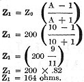
Solving for "Z1" the series element from equation (4).

"Z2" the shunt element is the same as for the H-type pad, as the formulas
from which "Z2" the shunt arm is determined, is the same for both H and
T-type pads. This is seen from inspection of the formulas for the two types of networks.
The completed network shown in Fig. 15, having the constants as determined
above, of "Z1" the series element equal to 164 ohms, and "Z2"
the shunt element equal to 40.4 ohms, when interposed between the two 200-ohm impedances,
will give the desired 20 decibel loss.
It will be noticed (see Fig. 15) that the series arm "Z1" as
determined for the T-type pad, is exactly twice the value found for "Z1"
in the H-type pad, and checks with the values given in Table 4, from which the constants
"Z1" and "Z2" for T-type pads may be found, when working between
200- 500- and 600-ohm impedances.
Design Information for Resistors Used in Attenuators

Fig. 15 (top) - A completed T-type network causing
a 20 db. loss.
Fig. 16 (bottom) - Illustrating a bifilar winding. A and
B are the ends of the winding.
The resistors used in attenuators must be non-reactive (have negligible inductance
and capacitance) so that the attenuator will maintain a constant impedance throughout
the audio band to the impedances between which it is working. By designing the attenuator
to have a constant impedance, it will offer the same degree of attenuation to all
audio frequencies, with the result that the frequency response characteristics of
the circuit will be practically flat, which is the ideal strived for in all voice
transmission circuits.
The following constructional data on the resistors used in attenuators is given,
so that the above mentioned characteristics may be obtained.
All resistors lower than 300 ohms are wound in bifilar fashion. The bifilar method
consists of paralleling the wire throughout the winding as shown in Fig. 16.
For all resistors below 300 ohms, the following accuracy limits for resistance
should be adhered to:

Resistors whose values are greater than 300 ohms, are wound in the well-known
reversed layer method, in which the layers are wound upon each other in reversed
directions.
For all resistors above 300 ohms, the follow-ing accuracy limits tor resistance
should be adhered to:

The inductance of a resistor is expressed in micro-henries, and the capacitance
of a resistor is expressed in micro-micro-farads.
The maximum allowable inductance in micro-henries for resistors below 1,000 ohms
is given in the following table.

The maximum allowable capacitance in micro-micro-farads for resistors above 1,000
is given below:

If the resistors are wound as specified, and the accuracy limits for resistance,
inductance, and capacity, as given above are maintained, a practically constant
impedance attenuator will be the result.
Posted November 14, 2023
(updated from original
post on 3/15/2017)
|


