Module 11 - Microwave Principles Pages
i,
1-1, 1-11,
1-21,
1-31,
1-41,
1-51,
1-61,
2-1,
2-11, 2-21,
2-31,
2-41,
2-51,
2-61,
3-1,
3-11,
AI-1,
Index-1,
Assignment 1,
Assignment 2
Because of the use of the decibel measurement system in the following paragraphs,
you will be introduced to it at this point. Technicians who deal with communications
and radar equipment most often speak of the gain of an amplifier or a system in terms
of units called DECIBELS (dB). Throughout your Navy career you will use decibels as
an indicator of equipment performance; therefore, you need to have a basic understanding
of the decibel system of measurement. Because the actual calculation of decibel measurements
is seldom required in practical applications, the explanation given in this module is
somewhat simplified. Most modern test equipment is designed to measure and indicate
decibels directly which eliminates the need for complicated mathematical calculations.
Nevertheless, a basic explanation of the decibel measurement system is necessary for
you to understand the significance of dB readings and equipment gain ratings which are
expressed in decibels.
| - |
Matter, Energy,
and Direct Current |
| - |
Alternating Current and Transformers |
| - |
Circuit Protection, Control, and Measurement |
| - |
Electrical Conductors, Wiring Techniques,
and Schematic Reading |
| - |
Generators and Motors |
| - |
Electronic Emission, Tubes, and Power Supplies |
| - |
Solid-State Devices and Power Supplies |
| - |
Amplifiers |
| - |
Wave-Generation and Wave-Shaping Circuits |
| - |
Wave Propagation, Transmission Lines, and
Antennas |
| - |
Microwave Principles |
| - |
Modulation Principles |
| - |
Introduction to Number Systems and Logic Circuits |
| - |
- Introduction to Microelectronics |
| - |
Principles of Synchros, Servos, and Gyros |
| - |
Introduction to Test Equipment |
| - |
Radio-Frequency Communications Principles |
| - |
Radar Principles |
| - |
The Technician's Handbook, Master Glossary |
| - |
Test Methods and Practices |
| - |
Introduction to Digital Computers |
| - |
Magnetic Recording |
| - |
Introduction to Fiber Optics |
| Note: Navy Electricity and Electronics Training
Series (NEETS) content is U.S. Navy property in the public domain. |
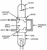
Figure 2-7A -
Functional and schematic diagram of a two-cavity klystron.
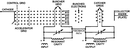
Figure 2-7B - Functional and schematic diagram of a two-cavity
klystron.
The function of the CATCHER GRIDS is to absorb energy from the electron beam.
The catcher
grids are placed along the beam at a point where the bunches are fully formed.
The location is determined by the transit time of the bunches at the natural resonant
frequency of the cavities (the resonant frequency of the catcher cavity is the same
as the buncher cavity). The location is chosen because maximum energy transfer to
the output (catcher) cavity occurs when the electrostatic field is of the correct
polarity to slow down the electron bunches.
The two-cavity klystron in figure 2-7A and B may be used either as an oscillator
or an amplifier. The configuration shown in the figure is correct for oscillator
operation. The feedback path provides energy of the proper delay and phase relationship
to sustain oscillations. a signal applied at the buncher grids will be amplified
if the feedback path is removed.
Q-11. What is the basic principle of operation of a klystron?
2-11
Q-12. The electrons in the beam of a klystron are speeded up by a high dc potential
applied to what elements?
Q-13. The two-cavity klystron uses what cavity as an output cavity?
Q-14. a two-cavity klystron without a feedback path will operate as what type
of circuit?
The Multicavity Power Klystron
Klystron amplification, power output, and efficiency can be greatly improved
by the addition of intermediate cavities between the input and output cavities
of the basic klystron. Additional cavities serve to velocity-modulate the
electron beam and produce an increase in the energy available at the output.
Since all intermediate cavities in a multicavity klystron operate in the same
manner, a representative THREE-CAVITY KLYSTRON will be discussed.
AAA three-cavity klystron is illustrated in figure 2-8. The entire DRIFT-TUBE
ASSEMBLY, the three CAVITIES, and the Collector PLATE of the three-cavity klystron
are operated at ground potential for reasons of safety. The electron beam is formed
and accelerated toward the drift tube by a large negative pulse applied to the cathode.
Magnetic FOCUS Coils are placed around the drift tube to keep the electrons in a
tight beam and away from the side walls of the tube. The focus of the beam is also
aided by the concave shape of the cathode in high-powered klystrons.
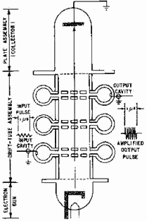
Figure 2-8 - Three-cavity klystron.
2-12
The output of any klystron (regardless of the number of cavities used) is developed
by velocity modulation of the electron beam. The electrons that are accelerated
by the cathode pulse are acted upon by RF fields developed across the input and
middle cavities. Some electrons are accelerated, some are decelerated, and some
are unaffected. Electron reaction depends on the amplitude and polarity of the fields
across the cavities when the electrons pass the cavity gaps. During the time the
electrons are traveling through the drift space between the cavities, the accelerated
electrons overtake the decelerated electrons to form bunches. As a result, bunches
of electrons arrive at the output cavity at the proper instant during each cycle
of the RF field and deliver energy to the output cavity.
Only a small degree of bunching takes place within the electron beam during the
interval of travel from the input cavity to the middle cavity. The amount of bunching
is sufficient, however, to cause oscillations within the middle cavity and to maintain
a large oscillating voltage across the input gap. Most of the velocity modulation
produced in the three-cavity klystron is caused by the voltage across the input
gap of the middle cavity. The high voltage across the gap causes the bunching process
to proceed rapidly in the drift space between the middle cavity and the output cavity.
The electron bunches cross the gap of the output cavity when the gap voltage is
at maximum negative. Maximum energy transfer from the electron beam to the output
cavity occurs under these conditions. The energy given up by the electrons is the
kinetic energy that was originally absorbed from the cathode pulse.
Klystron amplifiers have been built with as many as five intermediate cavities
in addition to the input and output cavities. The effect of the intermediate cavities
is to improve the electron bunching process which improves amplifier gain. The overall
efficiency of the tube is also improved to a lesser extent. Adding more cavities
is roughly the same as adding more stages to a conventional amplifier. The overall
amplifier gain is increased and the overall bandwidth is reduced if all the stages
are tuned to the same frequency. The same effect occurs with multicavity klystron
tuning. a klystron amplifier tube will deliver high gain and a narrow bandwidth
if all the cavities are tuned to the same frequency. This method of tuning is called
SYNCHRONOUS TUNING. If the cavities are tuned to slightly different frequencies,
the gain of the amplifier will be reduced but the bandwidth will be appreciably
increased. This method of tuning is called STAGGERED TUNING.
Q-15. What can be added to the basic two-cavity klystron to increase the amount
of velocity modulation and the power output?
Q-16. How is the electron beam of a three-cavity klystron accelerated toward
the drift tube?
Q-17. Which cavity of a three-cavity klystron causes most of the velocity modulation?
Q-18. In a multicavity klystron, tuning all the cavities to the same frequency
has what effect on the bandwidth of the tube?
Q-19. The cavities of a multicavity klystron are tuned to slightly different
frequencies in what method of tuning?
The Reflex Klystron
Another tube based on velocity modulation, and used to generate microwave energy,
is the REFLEX KLYSTRON (figure 2-9). The reflex klystron contains a Reflector PLATE,
referred to as the REPELLER, instead of the output cavity used in other types of
klystrons. The electron beam is modulated as it was in the other types of klystrons
by passing it through an oscillating resonant cavity, but here the similarity ends.
The feedback required to maintain oscillations within the cavity is obtained by
reversing the beam and sending it back through the cavity. The electrons in the
beam are velocity-modulated before the beam passes through the cavity the second
time and will give up the energy required to maintain
2-13
oscillations. The electron beam is turned around by a negatively charged electrode
that repels the beam. This negative element is the repeller mentioned earlier. This
type of klystron oscillator is called a reflex klystron because of the reflex action
of the electron beam.
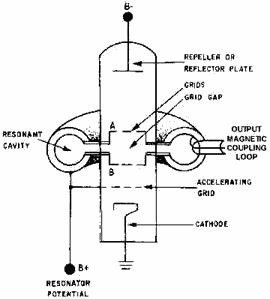
Figure 2-9 - Functional diagram of a reflex klystron.
Three power sources are required for reflex klystron operation: (1) filament
power, (2) positive resonator voltage (often referred to as beam voltage) used to
accelerate the electrons through the grid gap of the resonant cavity, and (3) negative
repeller voltage used to turn the electron beam around. The electrons are focused
into a beam by the electrostatic fields set up by the resonator potential (B+) in
the body of the tube. Note in figure 2-9 that the resonator potential is common
to the resonator cavity, the accelerating grid, and the entire body of the tube.
The resonator potential also causes the resonant cavity to begin oscillating
at its natural frequency when the tube is energized. These oscillations cause an
electrostatic field across the grid gap of the cavity that changes direction at
the frequency of the cavity. The changing electrostatic field affects the electrons
in the beam as they pass through the grid gap. Some are accelerated and some are
decelerated, depending upon the polarity of the electrostatic field as they pass
through the gap. Figure 2-10, view (A), illustrates the three possible ways an electron
can be affected as it passes through the gap (velocity increasing, decreasing, or
remaining constant). Since the resonant cavity is oscillating, the grid potential
is an alternating voltage that causes the electrostatic field between the grids
to follow a sine-wave curve as shown in figure 2-10, view (B). As a result, the
velocity of the electrons passing through the gap is affected uniformly as a function
of that sine wave. The amount of velocity change is dependent on the strength and
polarity of the grid voltage.
2-14
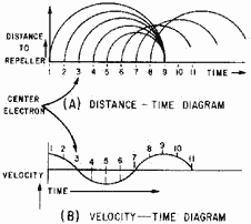
Figure 2-10 - Electron bunching diagram.
The variation in grid voltage causes the electrons to enter the space between
the grid and the repeller at various velocities. For example, in figure 2-10, views
(A) and (B), the electrons at times 1 and 2 are speeded up as they pass through
the grid. At time 3, the field is passing through zero and the electron is unaffected.
At times 4 and 5, the grid field is reversed; the electrons give up energy because
their velocity is reduced as they pass through the grids.
The distance the electrons travel in the space separating the grid and the repeller
depends upon their velocity. Those moving at slower velocities, such as the electron
at time 4, move only a short distance from the grid before being affected by the
repeller voltage. When this happens, the electron is forced by the repeller voltage
to stop, reverse direction, and return toward the grid. The electrons moving at
higher velocities travel further beyond the grid before reversing direction because
they have greater momentum. If the repeller voltage is set at the correct value,
the electrons will form a bunch around the constant-speed electrons. The electrons
will then return to the grid gap at the instant the electrostatic field is at the
correct polarity to cause maximum deceleration of the bunch. This action is also
illustrated in figure 2-10, view (A). When the grid field provides maximum deceleration,
the returning electrons release maximum energy to the grid field which is in phase
with cavity current. Thus, the returning electrons supply the regenerative feedback
required to maintain cavity oscillations.
The constant-speed electrons must remain in the reflecting field space for a
minimum time of 3/4 cycle of the grid field for maximum energy transfer. The period
of time the electrons remain in the epeller field is determined by the amount of
negative repeller voltage. The reflex klystron will continue to oscillate if the
electrons remain in the repeller field longer than 3/4 cycle (as long as the electrons
return to the grid gap when the field is of the proper polarity to decelerate the
electrons). Figure 2-11 shows the effect of the repeller field on the electron bunch
for 3/4 cycle and for 1 3/4 cycles. Although
not shown in the figure, the constant-velocity electrons may remain in the repeller
field for any number of cycles over the minimum 3/4 cycle. If the electrons remain
in the field for longer than 3/4 cycle, the difference in electron transit time causes the tube performance characteristics
to change. The differences in operating characteristics are identified by Modes
of Operation.
2-15
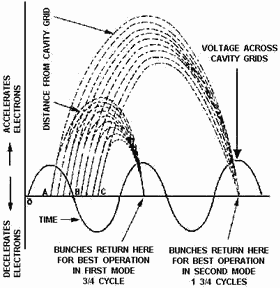
Figure 2-11 - Bunching action of a reflex klystron.
The reflex klystron operates in a different mode for each additional cycle that
the electrons remain in the repeller field. Mode 1 is obtained when the repeller
voltage produces an electron transit time of 3/4 cycle. Additional modes follow
in sequence. Mode 2 has an electron transit time of 1 3/4 cycles; mode 3 has an
electron transit time of 2 3/4 cycles; etc. The physical design of the tube limits
the number of modes possible in practical applications. a range of four modes of
operation are normally available. The actual mode used (1 3/4 cycles through 4 3/4
cycles, 2 3/4 cycles through 6 3/4 cycles, etc.) depends upon the application. The
choice of mode is determined by the difference in power available from each mode
and the band of frequencies over which the circuit can be tuned.
Output Power. - The variation in output power for different modes of operation
can be explained by examining the factors which limit the amplitude of oscillations.
Power and amplitude limitations are caused by the DEBUNCHING process of the electrons
in the repeller field space. Debunching is simply the spreading out of the electron
bunches before they reach electrostatic fields across the cavity grid . The lower
concentration of electrons in the returning bunches provides less power for delivery
to the oscillating cavity. This reduced power from the bunches, in turn, reduces
the amplitude of the cavity oscillations and causes a decrease in output power.
In higher modes of operation the electron bunches are formed more slowly. They are
more likely to be affected by debunching because of mutual repulsion between the
negatively charged electrons. The long drift time in the higher modes allows more
time for this electron interaction and, as a result, the effects of debunching are
more severe. The mutual repulsion changes the relative velocity between the electrons
in the bunches and causes the bunches to spread out.
2-16
Figure 2-12 illustrates the ELECTRONIC TUNING (tuning by altering the repeller
voltage) range and output power of a reflex klystron. Each mode has a center frequency
of 3,000 megahertz which is predetermined by the physical size of the cavity. The
output power increases as the repeller voltage is made more negative. This is because
the transit time of the electron bunches is decreased.
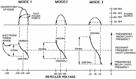
Figure 2-12 - Electronic tuning and output power of a reflex klystron.
Electronic tuning does not change the center frequency of the cavity, but does
vary the frequency within the mode of operation. The amount the frequency can be
varied above or below the center frequency is limited by the half-power points of
the mode, as shown in figure 2-12. The center frequency can be changed by one of
two methods One method, GRID-GAP TUNING, varies the cavity frequency by altering
the distance between the grids to change the physical size of the cavity. This method
varies the capacitance of the cavity by using a tuning screw to change the distance
between the grids mechanically. The cavity can also be tuned by PADDLES or SLUGS
that change the inductance of the cavity.
Q-20. What element of the reflex klystron replaces the output cavity of a normal
klystron?
Q-21. When the repeller potential is constant, what property of the electron
determines how long it will remain in the drift space of the reflex klystron?
Q-22. The constant-speed electrons of an electron bunch in a reflex klystron
must remain in the repeller field for what minimum time?
Q-23. If the constant-speed electrons in a reflex klystron remain in the repeller
field for 1 3/4 cycles, what is the mode of operation?
2-17
Q-24. Debunching of the electron bunches in the higher modes of a reflex klystron
has what effect on output power?
Q-25. What limits the tuning range around the center frequency of a reflex klystron
in a particular mode of operation?
The Decibel Measurement System
Because of the use of the decibel measurement system in the following paragraphs,
you will be introduced to it at this point. Technicians who deal with communications
and radar equipment most often speak of the gain of an amplifier or a system in terms
of units called DECIBELS (dB). Throughout your Navy career you will use decibels as
an indicator of equipment performance; therefore, you need to have a basic understanding
of the decibel system of measurement. Because the actual calculation of decibel measurements
is seldom required in practical applications, the explanation given in this module is
somewhat simplified. Most modern test equipment is designed to measure and indicate
decibels directly which eliminates the need for complicated mathematical calculations.
Nevertheless, a basic explanation of the decibel measurement system is necessary for
you to understand the significance of dB readings and equipment gain ratings which are
expressed in decibels.
The basic unit of measurement in the system is not the decibel, but the bel,
named in honor of the American inventor, Alexander Graham Bell. The bel is a unit
that expresses the logarithmic ratio between the input and output of any given component,
circuit, or system and may be expressed in terms of voltage, current, or power.
Most often it is used to show the ratio between input and output power. The formula
is as follows:

The gain of an amplifier can be expressed in bels by dividing the output (P1)
by the input (P2) and taking the base 10 logarithm of the resulting quotient. Thus,
if an amplifier doubles the power, the quotient will be 2. If you consult a logarithm
table, you will find that the base 10 logarithm of 2 is 0.3; so the power gain of
the amplifier is 0.3 bel. Experience has taught that because the bel is a rather
large unit, it is difficult to apply. a more practical unit that can be applied
more easily is the decibel (1/10 bel). Any figure expressed in bels can easily be
converted to decibels by multiplying the figure by 10 or simply by moving the decimal
one place to the right. The previously found ratio of 0.3 is therefore equal to
3 decibels.
The reason for using the decibel system when expressing signal strength may be
seen in the power ratios in table 2-1. For example, to say that a reference signal
has increased 50 dB is much easier than to say the output has increased 100,000
times. The amount of increase or decrease from a chosen reference level is the basis
of the decibel measurement system, not the reference level itself. Whether the input
power is increased from 1 watt to 100 watts or from 1,000 watts to 100,000 watts,
the amount of increase is still 20 decibels.
2-18
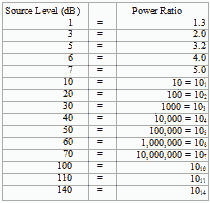
Table 2-1 - Decibel Power Ratios
Examine table 2-1 again, and take particular note of the power ratios for source
levels of 3 dB and 6 dB. As the table illustrates, an increase of 3 dB represents
a doubling of power. The reverse is also true. If a signal decreases by 3 dB, half
the power is lost. For example, a 1,000 watt signal decreased by 3 dB will equal
500 watts while a 1,000 watt signal increased by 3 dB equals 2,000 watts.
The attenuator is a widely used piece of test equipment that can be used to demonstrate
the importance of the decibel as a unit of measurement. Attenuators are used to
reduce a signal to a smaller level for use or measurement. Most attenuators are
rated by the number of decibels the signal is reduced. The technician's job is to
know the relationship between the dB rating and the power reduction it represents.
This is so important, in fact, that every student of electronics should memorize
the relationships in table 2-1 through the 60 dB range. The technician will have
to apply this knowledge to prevent damage to valuable equipment. a helpful hint
is to note that the first digit of the source level (on the chart) is the same number
as the corresponding power of 10 exponent; i.e., 40 dB = 1 x 10⁴ or 10,000.
a 20 dB attenuator, for example, will reduce an input signal by a factor of 100.
In other words, a 100- milliwatt signal will be reduced to 1 milliwatt. a 30 dB
attenuator will reduce the same 100-milliwatt signal by a factor of 1,000 and produce
an output of 0.1 milliwatt. When an attenuator of the required size is not available,
attenuators of several smaller sizes may be added directly together to reach the
desired amount of attenuation. a 10 dB attenuator and a 20 dB attenuator add directly
to equal 30 dB of attenuation. The same relationship exists with amplifier stages
as well. If an amplifier has two stages rated at 10 dB each, the total amplifier
gain will be 20 dB.
When you speak of the dB level of a signal, you are really speaking of a logarithmic
comparison between the input and output signals. The input signal is normally used
as the reference level. However, the application sometimes requires the use of a
standard reference signal. The most widely used reference level is a 1-milliwatt
signal. The standard decibel abbreviation of dB is changed to dBm to indicate the
use of the 1-milliwatt standard reference. Thus, a signal level of +3 dBm is 3 dB
above 1 milliwatt, and a signal level of -3 dBm is 3 dB below 1 milliwatt. Whether
using dB or dBm, a plus (+) sign (or no sign at all) indicates the output signal
is larger than the reference; a minus (-) sign indicates the output signal is less
than the reference.
2-19
The Navy student of electronics will encounter the dBm system of measurement
most often as a figure indicating the receiver sensitivity of radar or communications
equipment. Typically, a radar receiver will be rated at approximately -107 dBm,
which means the receiver will detect a signal 107 dB below 1 milliwatt.
The importance of understanding the decibel system of measurement can easily
be seen in the case of receiver-sensitivity measurements. At first glance a loss
of 3 dBm from a number as large as -107 dBm seems insignificant; however, it becomes
extremely important when the number indicates receiver sensitivity in the decibel
system. When the sensitivity falls to -104 dBm, the receiver will only detect a
signal that is twice as large as a signal at -107 dBm.
The Traveling-Wave Tube
The Traveling-Wave Tube (TWT) is a high-gain, low-noise, wide-bandwidth microwave
amplifier. It is capable of gains greater than 40 dB with bandwidths exceeding an
octave. (A bandwidth of
1 octave is one in which the upper frequency is twice the lower frequency.) Traveling-wave
tubes have
been designed for frequencies as low as 300 megahertz and as high as 50 gigahertz.
The TWT is primarily a voltage amplifier. The wide-bandwidth and low-noise characteristics
make the TWT ideal for use as an RF amplifier in microwave equipment.
The physical construction of a typical TWT is shown in figure 2-13. The TWT contains
an electron gun which produces and then accelerates an electron beam along the axis
of the tube. The surrounding magnet provides a magnetic field along the axis of
the tube to focus the electrons into a tight beam. The Helix, at the center of the
tube, is a coiled wire that provides a low-impedance transmission line for the RF
energy within the tube. The RF input and output are coupled onto and removed from
the helix by directional couplers that have no physical connection to the helix.
If the RF energy is transported on coaxial cables, the coaxial couplers are wound
in a helical manner similar to that shown in figure 2-13. If the RF energy is transported
in waveguides, waveguide directional couplers are used. The attenuator prevents
any reflected waves from traveling back down the helix.
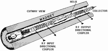
Figure 2-13 - Physical construction of a TWT.
A simplified version of TWT operation is shown in figure 2-14. In the figure,
an electron beam is passing along a nonresonant transmission line represented by
a straight wire. The input to the transmission line is an RF wave which travels
on the line from input to output. The line will transport a
2-20
|