Module 11 - Microwave Principles Pages
i,
1-1, 1-11,
1-21,
1-31,
1-41,
1-51,
1-61,
2-1,
2-11, 2-21,
2-31,
2-41,
2-51,
2-61,
3-1,
3-11,
AI-1,
Index-1,
Assignment 1,
Assignment 2
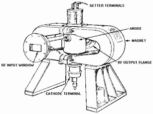
Figure 2-38. - Crossed-field amplifier (Amplitron). Q-44. Why is the pi mode the most commonly used magnetron mode of operation? Q-45. What two methods are used to couple energy into and out of magnetrons? Q-46. Magnetron tuning by altering the surface-to-volume
ratio of the hole portion of a hole-and-slot cavity is what type of tuning? Q-47. Capacitive tuning by
inserting a ring into the cavity slot of a magnetron is accomplished by what type of tuning mechanism?
SOLID-STATE Microwave DEVICES As with vacuum tubes, the special electronics effects
encountered at microwave frequencies severely limit the usefulness of transistors in most circuit applications.
The need for small-sized microwave devices has caused extensive research in this area. This research has produced
solid-state devices with higher and higher frequency ranges. The new solid-state microwave devices are
predominantly active, two-terminal diodes, such as tunnel diodes, varactors, transferred-electron devices, and
avalanche transit- time diodes. This section will describe the basic theory of operation and some of the
applications of these relatively new solid-state devices.
Tunnel Diode Devices The TUNNEL DIODE is a PN junction with a very high
concentration of impurities in both the p and n regions. The high concentration of impurities causes it to exhibit
the properties of a negative-resistance element over part of its range of operation, as shown in the
characteristic curve in figure 2-39. In other words, the resistance to current flow through the tunnel diode
increases as the applied voltage increases over a portion of its region of operation. Outside the
negative-resistance region, the tunnel diode functions essentially the same as a normal diode. However, the very
high impurity density causes a junction depletion region so narrow that both holes and electrons can transfer
across the PN junction by a quantum 2-41
mechanical action called TUNNELING. Tunneling causes the negative-resistance action and is so fast
that no transit-time effects occur even at microwave frequencies. The lack of a transit-time effect permits the use of tunnel diodes in a wide variety of microwave circuits, such as amplifiers, oscillators, and switching
devices. The detailed theory of tunnel-diode operation and the negative-resistance property exhibited by the
tunnel diode was discussed in NEETS, Module 7, Introduction to Solid-State Devices and Power Supplies, Chapter 3.
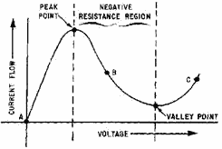
Figure 2-39. - Tunnel-diode characteristic curve. TUNNEL-DIODE Oscillators. - a tunnel diode, biased at the center point of the negative-
resistance range (point B in figure 2-39) and coupled to a tuned circuit or cavity, produces a very stable
oscillator. The oscillation frequency is the same as the tuned circuit or cavity frequency. Microwave
tunnel-diode oscillators are useful in applications that require microwatts or, at most, a few milliwatts of
power, such as local oscillators for microwave superheterodyne receivers. Tunnel-diode oscillators can be
mechanically or electronically tuned over frequency ranges of about one octave and have a top-end frequency limit
of approximately 10 gigahertz. Tunnel-diode oscillators that are designed to operate at microwave
frequencies generally use some form of transmission line as a tuned circuit. Suitable tuned circuits can be built
from coaxial lines, transmission lines, and waveguides. An example of a highly stable tunnel-diode oscillator is shown in figure 2-40. a tunnel-diode is loosely
coupled to a high-Q tunable cavity. Loose coupling is achieved by using a short, antenna feed probe placed
off-center in the cavity. Loose coupling is used to increase the stability of the oscillations and the output
power over a wider bandwidth.
2-42
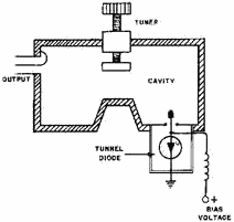
Figure 2-40. - Tunnel-diode oscillator. The output power produced is in the range of a few hundred microwatts, sufficient for many microwave
applications. The frequency at which the oscillator operates is determined by the physical positioning of the
tuner screw in the cavity. Changing the output frequency by this method is called MECHANICAL TUNING. In addition
to mechanical tuning, tunnel-diode oscillators may be tuned electronically. One method is called BIAS TUNING and
involves nothing more than changing the bias voltage to change the bias point on the characteristic curve of the
tunnel-diode. Another method is called VARACTOR TUNING and requires the addition of a varactor to the basic
circuit. Varactors were discussed in NEETS, Module 7, Introduction to Solid-State Devices, and Power Supplies,
Chapter 3. Tuning is achieved by changing the voltage applied across the varactor which alters the capacitance of
the tuned circuit. TUNNEL-DIODE AmplifierS. - Low-noise, tunnel-diode amplifiers represent an important microwave
application of tunnel diodes. Tunnel-diode amplifiers with frequencies up to 85 gigahertz have been built in
waveguides, coaxial lines, and transmission lines. The low-noise generation, gain ratios of up to 30 dB, high
reliability, and light weight make these amplifiers ideal for use as the first stage of amplification in
communications and radar receivers.
Most microwave tunnel-diode amplifiers are REFLECTION-TYPE, CIRCULATOR-COUPLED AmplifierS. As in
oscillators, the tunnel diode is biased to the center point of its negative-resistance region, but a CIRCULATOR
replaces the tuned cavity. A circulator is a waveguide device that allows energy to travel in one
direction only, as shown in figure 2-41. The tunnel diode in figure 2-41 is connected across a tuned-input
circuit. This arrangement normally produces feedback that causes oscillations if the feedback is allowed to
reflect back to the tuned- input circuit. The feedback is prevented because the circulator carries all excess
energy to the absorptive load (R L). In this configuration the tunnel diode cannot oscillate, but will amplify. 2-43
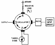
Figure 2-41. - Tunnel-diode amplifier. The desired frequency input signal is fed to port 1 of the circulator through a bandpass filter. The
filter serves a dual purpose as a bandwidth selector and an impedance-matching device that improves the gain of
the amplifiers. The input energy enters port 2 of the circulator and is amplified by the tunnel diode. The
amplified energy is fed from port 2 to port 3 and on to the mixer. If any energy is reflected from port 3, it is
passed to port 4, where it is absorbed by the matched load resistance. TUNNEL-DIODE Frequency
CONVERTERS and MIXERS. - Tunnel diodes make excellent mixers and frequency converters because their
current-voltage characteristics are highly nonlinear. While other types of frequency converters usually have a
conversion power loss, tunnel-diode converters can actually have a conversion power gain. a single tunnel diode
can also be designed to act as both the nonlinear element in a converter and as the negative-resistance element in
a local oscillator at the same time. Practical tunnel-diode frequency converters usually have either a
unity conversion gain or a small conversion loss. Conversion gains as high as 20 dB are possible if the tunnel
diode is biased near or into the negative-resistance region. Although high gain is useful in some applications, it
presents problems in stability. For example, the greatly increased sensitivity to variations in input impedance
can cause high- gain converters to be unstable unless they are protected by isolation circuitry. As with
tunnel-diode amplifiers, low-noise generation is one of the more attractive characteristics of tunnel-diode
frequency converters. Low-noise generation is a primary concern in the design of today's extremely sensitive
communications and radar receivers. This is one reason tunnel-diode circuits are finding increasingly wide
application in these fields. Q-48. Name the procedure used to reduce excessive arcing in a magnetron?
Q-49. What causes the negative-resistance property of tunnel diodes? Q-50. What determines the
frequency of a tunnel-diode oscillator? Q-51. Why is the tunnel diode loosely coupled to the cavity in a
tunnel-diode oscillator? Q-52. What is the purpose of the circulator in a tunnel-diode amplifier?
2-44
Varactor Devices The VARACTOR is another of the active two-terminal diodes
that operates in the microwave range. Since the basic theory of varactor operation was presented in NEETS, Module
7, Introduction to Solid- State Devices and Power Supplies, Chapter 3, only a brief review of the basic principles
is presented here.
The varactor is a semiconductor diode with the properties of a voltage-dependent capacitor. Specifically,
it is a variable-capacitance, PN-junction diode that makes good use of the voltage dependency of the
depletion-area capacitance of the diode. In figure 2-42A, two materials are brought together to form a
PN-junction diode. The different energy levels in the two materials cause a diffusion of the holes and electrons
through both materials which tends to balance their energy levels. When this diffusion process stops, the diode is
left with a small area on either side of the junction, called the depletion area, which contains no free electrons
or holes. The movement of electrons through the materials creates an electric field across the depletion area that
is described as a barrier potential and has the electrical characteristics of a charged capacitor.
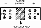
Figure 2-42A. - PN-junction diode as a variable capacitor. External bias, applied in either the forward or reverse direction, as shown in figure 2-42B and C,
affects the magnitude, barrier potential, and width of the depletion area. Enough forward or reverse bias will
overcome the barrier potential and cause current to flow through the diode. The width of the depletion region can
be controlled by keeping the bias voltage at levels that do not allow current flow. Since the depletion area acts
as a capacitor, the diode will perform as a variable capacitor that changes with the applied bias voltage. The
capacitance of a typical varactor can vary from 2 to 50 picofarads for a bias variation of just 2 volts. 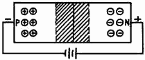
Figure 2-42B. - PN-junction diode as a variable capacitor.
2-45
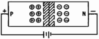
Figure 2-42C. - PN-junction diode as a variable capacitor. The variable capacitance property of the varactor allows it to be used in circuit applications, such as
amplifiers, that produce much lower internal noise levels than circuits that depend upon resistance properties.
Since noise is of primary concern in receivers, circuits using varactors are an important development in the field
of low-noise amplification. The most significant use of varactors to date has been as the basic component in
parametric amplifiers. PARAMETRIC AmplifierS. - The parametric amplifier is named for the
time-varying parameter, or value of capacitance, associated with the operation. Since the underlying principle of
operation is based on reactance, the parametric amplifier is sometimes called a REACTANCE Amplifier. The
conventional amplifier is essentially a variable resistance that uses energy from a dc source to increase ac
energy. The parametric amplifier uses a nonlinear variable reactance to supply energy from an ac source to a load.
Since reactance does not add thermal noise to a circuit, parametric amplifiers produce much less noise than most
conventional amplifiers. Because the most important feature of the parametric amplifier is the low-noise
characteristic, the nature of ELECTRONIC NOIsE and the effect of this type of noise on receiver operation must
first be discussed. Electronic noise is the primary limitation on receiver sensitivity and is the name given to
very small randomly fluctuating voltages that are always present in electronic circuits. The sensitivity limit of
the receiver is reached when the incoming signal falls below the level of the noise generated by the receiver
circuits. At this point the incoming signal is hidden by the noise, and further amplification has no effect
because the noise is amplified at the same rate as the signal. The effects of noise can be reduced by careful
circuit design and control of operating conditions, but it cannot be entirely eliminated. Therefore, circuits such
as the parametric amplifier are important developments in the fields of communication and radar. The basic
theory of parametric amplification centers around a capacitance that varies with time. Consider the simple series
circuit shown in figure 2-43. When the switch is closed, the capacitor charges to value (Q). If the switch is
opened, the isolated capacitor has a voltage across the plates determined by the charge Q divided by the
capacitance C. 2-46
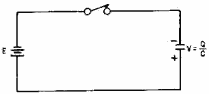
Figure 2-43. - Voltage amplification from a varying capacitor. An increase in the charge Q or a decrease in the capacitance C causes an increase in the voltage across
the plates. Thus, a voltage increase, or amplification, can be obtained by mechanically or electronically varying
the amount of capacitance in the circuit. In practice a voltage-variable capacitance, such as a varactor, is used.
The energy required to vary the capacitance is obtained from an electrical source called a PUMP. Figure
2-44, view (A), shows a circuit application using a voltage-variable capacitor and a pump circuit. The pump
circuit decreases the capacitance each time the input signal (E) across the capacitor reaches maximum. The
decreased capacitance causes a voltage buildup as shown by the dotted line in view (B). Therefore, each time the
pump decreases capacitance (view (C)), energy transfers from the pump circuit to the input signal. The
step-by-step buildup of the input-signal energy level is shown in view (D).

Figure 2-44. - Energy transfer from pump signal to input signal.
2-47
Proper phasing between the pump and the input signal is crucial in this circuit. The electrical pump
action is simply a sine-wave voltage applied to a varactor located in a resonant cavity. For proper operation, the
capacitance must be decreased when the input voltage is maximum and increased when the input voltage is minimum.
In other words, the pump signal frequency must be exactly double the frequency of the input signal. This
relationship can be seen when you compare views (B) and (C). a parametric amplifier of the type shown in figure
2-44 is quite phase-sensitive. The input signal and the capacitor variation are often in the wrong phase for long
periods of time. A parametric amplifier that is not phase-sensitive, referred to as a NONDegenerative
PARAMETRIC Amplifier, uses a pump circuit with a frequency higher than twice the input signal. The
higher-frequency pump signal mixes with the input signal and produces additional frequencies that represent both
the sum and difference of the input signal and pump frequencies.
Figure 2-45A, is a diagram of a typical nondegenerative parametric amplifier with the equivalent circuit
shown in figure 2-45B. The pump signal (fp) is applied to the varactor. The cavity on the left is resonant at the
input frequency (fs), and the cavity on the right is resonant at the difference frequency (fp-fs). The difference
frequency is called the IDLER- or LowER-SIDEBand frequency. The varactor is located at the high-voltage points of
the two cavities and is reverse biased by a small battery. The pump signal varies the bias above and below the
fixed-bias level. 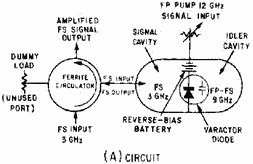
Figure 2-45A. - Nondegenerative parametric amplifier. Circuit. 2-48
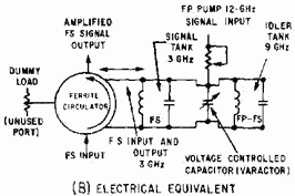
Figure 2-45B. - Nondegenerative parametric amplifier. ELECTRICAL EQUIVALENT. The pump signal causes the capacitor in figure 2-45A to vary at a 12-gigahertz rate. The 3-gigahertz
input signal enters via a four-port ferrite circulator, is developed in the signal cavity, and applied across the
varactor. The nonlinear action of the varactor produces a 9-gigahertz difference frequency (fp-fs) with an
energy-level higher than the original input signal. The difference (idler) frequency is reapplied to the
varactor to increase the gain and to produce an output signal of the correct frequency. The 9-gigahertz idler
frequency recombines with the 12-gigahertz pump signal and produces a 3-gigahertz difference signal that has a
much larger amplitude than the original 3-gigahertz input signal. The amplified signal is sent to the ferrite
circulator for transfer to the next stage. As with tunnel-diode amplifiers, the circulator improves
stability by preventing reflection of the signal back into the amplifier. Reflections would be amplified and cause
uncontrollable oscillations. The ferrite circulator also serves as an isolator to prevent source and load
impedance changes from affecting gain. Typically, the gain of a parametric amplifier is about 20 dB. The
gain can be controlled with a variable attenuator that changes the amount of pump power applied to the varactor. Parametric amplifiers are relatively simple in construction. The only component is a varactor diode placed in an
arrangement of cavities and waveguides. The most elaborate feature of the amplifier is the mechanical tuning
mechanism. Figure 2-46 illustrates an actual parametric amplifier.
2-49
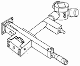
Figure 2-46. - Parametric amplifier. PARAMETRIC Frequency CONVERTERS. - Parametric frequency converters, using varactors, are
of three basic types. The Upper-SIDEBand PARAMETRIC UP-CONVERTER produces an output frequency that is the SUM of
the input frequency and the pump frequency. The LowER-SIDEBand PARAMETRIC DOWN-CONVERTER produces an output
frequency that is the Difference between the pump frequency and the input frequency. The DOUBLE-SIDEBand
PARAMETRIC UP-CONVERTER produces an output in which both the SUM and the Difference of the pump and input
frequencies are available. Parametric frequency converters are very similar to parametric amplifiers in both
construction and operation. Figure 2-47 is a functional diagram of a parametric down-converter. The
parametric frequency converter operates in the same manner as the parametric amplifier except that the sideband
frequencies are not reapplied to the varactor. Therefore, the output is one or both of the sideband frequencies
and is not the same as the input frequency. The output frequency is determined by the cavity used as an output.
For example, the idler cavity in figure 2-47 could be replaced by a cavity that is resonant at the upper-sideband
frequency (22 gigahertz) to produce an upper-sideband parametric up-converter. Since input and output signals are
at different frequencies, the parametric frequency converter does not require a ferrite circulator. However, a
ferrite isolator is used to isolate the converter from changes in source impedance.

Figure 2-47. - Lower-sideband parametric down-converter.
2-50
| - |
Matter, Energy,
and Direct Current |
| - |
Alternating Current and Transformers |
| - |
Circuit Protection, Control, and Measurement |
| - |
Electrical Conductors, Wiring Techniques,
and Schematic Reading |
| - |
Generators and Motors |
| - |
Electronic Emission, Tubes, and Power Supplies |
| - |
Solid-State Devices and Power Supplies |
| - |
Amplifiers |
| - |
Wave-Generation and Wave-Shaping Circuits |
| - |
Wave Propagation, Transmission Lines, and
Antennas |
| - |
Microwave Principles |
| - |
Modulation Principles |
| - |
Introduction to Number Systems and Logic Circuits |
| - |
- Introduction to Microelectronics |
| - |
Principles of Synchros, Servos, and Gyros |
| - |
Introduction to Test Equipment |
| - |
Radio-Frequency Communications Principles |
| - |
Radar Principles |
| - |
The Technician's Handbook, Master Glossary |
| - |
Test Methods and Practices |
| - |
Introduction to Digital Computers |
| - |
Magnetic Recording |
| - |
Introduction to Fiber Optics |
| Note: Navy Electricity and Electronics Training
Series (NEETS) content is U.S. Navy property in the public domain. |
|