| - |
Matter, Energy,
and Direct Current |
| - |
Alternating Current and Transformers |
| - |
Circuit Protection, Control, and Measurement |
| - |
Electrical Conductors, Wiring Techniques,
and Schematic Reading |
| - |
Generators and Motors |
| - |
Electronic Emission, Tubes, and Power Supplies |
| - |
Solid-State Devices and Power Supplies |
| - |
Amplifiers |
| - |
Wave-Generation and Wave-Shaping Circuits |
| - |
Wave Propagation, Transmission Lines, and
Antennas |
| - |
Microwave Principles |
| - |
Modulation Principles |
| - |
Introduction to Number Systems and Logic Circuits |
| - |
- Introduction to Microelectronics |
| - |
Principles of Synchros, Servos, and Gyros |
| - |
Introduction to Test Equipment |
| - |
Radio-Frequency Communications Principles |
| - |
Radar Principles |
| - |
The Technician's Handbook, Master Glossary |
| - |
Test Methods and Practices |
| - |
Introduction to Digital Computers |
| - |
Magnetic Recording |
| - |
Introduction to Fiber Optics |
| Note: Navy Electricity and Electronics Training
Series (NEETS) content is U.S. Navy property in the public domain. |
NEETS Module 17 - Radio-Frequency Communications Principles
Pages i,
1-1,
1-11,
2-1,
2-11,
2-21,
2-31,
3-1,
3-11,
3-21,
3-31,
3-41,
4-1- to 4-10,
4-11,
5-1,
5-11, Index
controlled degenerative feedback. use of an npn transistor, in the same configuration,
would require the AGC voltage to possess a negative potential.
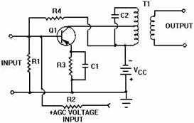
Figure 2-17. - Common emitter amplifier with AGC.
forWARD and REVERSE AGC. - When we use an AGC voltage to cause
degeneration by driving the amplifiers toward cutoff, it is referred to as REVERSE
AGC. Figure 2-18 shows the type of AGC circuitry normally used with this method.
a second method that uses AGC is an application called forWARD AGC. In the case
of forward AGC, you'll find the amplifier is driven toward the saturation region
of its characteristic curve. (Sometimes referred to as an energy diagram.)
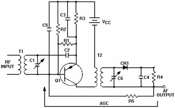
Figure 2-18. - Reverse AGC.
Let's look at our example. Assume the AGC voltage is negative. Under this condition,
Q1 is self biased; under no-signal conditions, it is operating well up on its characteristic
curve. When a signal is applied, negative AGC voltage is developed in the detector
circuit and fed back to Q1, which increases
2-21
forward bias. Any increase in signal level causes an increase in AGC voltage.
An increase in AGC voltage increases conduction, which in turn drives the transistor
to or near saturation. As the transistor approaches saturation, its gain is correspondingly
reduced.
On the other hand, if the input signal level decreases, the negative AGC voltage
decreases. The forward bias is then reduced, and the transistor operates on a lower
portion of its characteristic curve where gain is higher.
Forward AGC provides you with better signal-handling capabilities; however, reverse
AGC is simpler to use, causes less loading of the tuned circuits, and produces smaller
variations in input and output capacitance.
Q17. What does manual gain control do to strong and weak signals,
respectively?
Q18. What is the purpose of AGC/avc in a receiver?
Delayed Automatic Gain Control
The disadvantage of automatic gain control, attenuating even the weak signal,
is overcome by the use of delayed automatic gain control (DAGC). Let's take a look
at the typical DAGC circuitry in figure 2-19. This type of system develops no AGC
feedback until an established received signal strength is attained. For signals
weaker than this value, no AGC is developed. For sufficiently strong signals, the
delayed AGC circuit operates essentially the same as ordinary AGC.
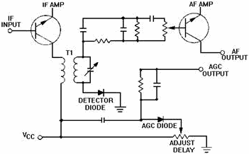
Figure 2-19. - Delayed AGC action.
Our circuit uses two separate diodes; one is the detector diode and the other
the AGC diode. The AGC diode is connected to the primary of the last IF transformer
and the detector diode to its secondary. a positive bias is applied to the cathode
of the AGC diode. This keeps it from conducting until a prearranged signal level
has been reached. The adjust delay control allows manual control of the AGC diode
bias. Manual control allows you to select the signal level at which AGC is applied.
If mostly weak stations are to
2-22
be received, the setting should be high (no AGC until the signal level is high).
However, you should set it as low as possible to prevent overloading of the last
IF amplifier by stronger signals.
Finally, you must have two diodes to obtain delayed AGC. If only one diode were used, the AGC would be developed from the detector diode, and there would be no
delayed action. Or, if a signal diode were biased to provide the delaying action
desired, no signal would pass to the audio amplifier until the bias was exceeded
by the input signal.
Beat-Frequency Oscillator
The beat-frequency oscillator (BFO) is necessary when you want to receive CW
signals. CW signals are not modulated with an audio component, you remember, so
we must provide one. The action of the RF amplifier, mixer, local oscillator, and
IF amplifier is the same for both CW and AM; but the CW signal reaches the detector
as a single frequency signal with no sideband components. To produce an AF output,
you must heterodyne (beat) any CW signal with an RF signal of the proper frequency.
This separate signal is obtained from an oscillator known as a beat-frequency oscillator.
Figure 2-20 is a block diagram of a superheterodyne receiver capable of receiving
and demodulating a CW signal. The BFO heterodynes at the detector and produces an
AF output. The detector (second detector) is used primarily because the mixer (first
detector) is normally used as the source of AGC.
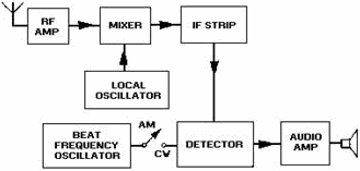
Figure 2-20. - Placement of the beat frequency oscillator.
If the intermediate frequency is 455 kilohertz and the BFO is tuned to 456 kilohertz
or 454 kilohertz, the difference frequency of 1 kilohertz is heard in the output.
Generally, you will tune the BFO from the front panel of a receiver. When you vary
the BFO control, you are varying the output frequency of the BFO and will hear changes
in the tone of the output audio signal.
Squelch
The sensitivity of a receiver is maximum when no signal is being received. This
condition occurs, for example, when a receiver is being tuned between stations.
At this time background noise is picked up by the antenna, and you will hear noise
greatly amplified. This noise is highly annoying and occurs because receiver gain
is maximum without a signal. You can often overcome this problem by using a circuit
called a SQUELCH, NOIsE SILENCER, NOIsE SUPPRESSOR, or NOIsE LIMITER. All of these
noise type circuits just clip the peaks of the noise spikes. Squelch will actually
eliminate noise. Figure 2-21 is a
2-23
typical circuit of this type. The circuit cuts off receiver output when no input
signal is being received. It accomplishes this by blocking either the detector or
audio amplifier when no signal is present. Let's take a look at the theory involved
in this process.
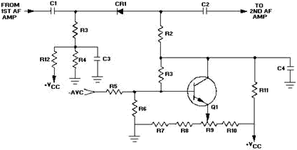
Figure 2-21. - Squelch circuit.
The squelch diode CR1 connects the output of the first AF stage to the input
of the second. Amplifier Q1 serves as the control transistor for the circuit. The
anode and cathode voltages of CR1 are normally biased positive with respect to ground.
With no input signal, R9 is adjusted until Q1 draws enough collector current
to reduce its collector voltage and the anode voltage of CR1 to a value below the
voltage on the cathode of CR1. At this point the anode voltage of the squelch diode
is negative with respect to its cathode, and conduction ceases. Audio output is
now reduced to zero and the receiver is silent.
The base of Q1 is connected to the automatic volume control (AVC) line. Anytime
a signal enters the receiver, a negative AVC voltage is applied to the base of Q1.
This reduces the collector current and increases the collector voltage, which in
turn increases the anode voltage of CR1 until the anode becomes positive with respect
to the cathode. Once again diode CR1 will conduct, and the signal will be passed
to the second AF amplifier. Diode CR1 is effectively a switch controlled by the
AVC voltage.
Q19. What is a disadvantage of AGC?
Q20. What is the main difference between AGC and DAGC?
Q21. What is the function of the BFO?
Q22. What is the purpose of a squelch circuit?
2-24
Audio Tone
The tone of the sound reproduced in the audio section of a receiver depends on
several factors. The frequency response of the audio amplifiers determines the degree
of amplification provided to different frequencies in the sound spectrum. The size
and quality of any loudspeaker used will determine its response to various frequencies.
Response of the human ear is the final judge of tonal quality, and that varies with
the individual.
Because of these variables, some form of tone control is sometimes used in Navy
receivers. Treble tones are defined as the audio frequencies above approximately
3,000 hertz and bass tones are those below approximately 300 hertz. Although several
methods of tone control can be used, we are only going to mention the attenuation
method. With this method, a decrease in the intensity of one tone can produce an
apparent increase in the intensity of another tone. As an example, let's look at
tones of 400 and 4,000 hertz produced by a speaker with the same intensity. If we
reduce the intensity of the 4,000-hertz tone, the 400-hertz tone will appear to
be louder, even though its intensity has not actually changed. You should see from
this example that bass emphasis can be accomplished by attenuating treble tones.
The simplest type of tone control is illustrated in figure 2-22. Fixed capacitor
C1 parallels the primary winding of the output transformer, effectively shunting
the higher frequencies to ground. The size of C1 determines the lowest frequency
to be affected. When you select the BASS position of the tone control, C1 is connected
and improves bass response by de-emphasizing the treble tones. You can often use
this circuit to improve the output of a small speaker with poor treble response.
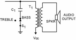
Figure 2-22. - Fixed capacitor tone control.
A continuously variable tone control is illustrated in figure 2-23. Tone control
R1 and bypass capacitor C1 act as a variable RC filter. With the wiper arm of R1
in the upper (BASS) position, C1 bypasses the higher frequencies to ground and provides
better bass response. When the wiper arm of R1 is in the lower (TREBLE) position,
the resistance of R1 is placed in series with C1, which reduces the shunting effect
of C1 to high frequencies and improves the treble response. This method gives you
the advantage of smooth, continuous tone control at all points between maximum bass
and maximum treble response.
2-25
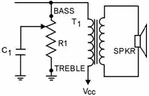
Figure 2-23. - Variable tone control using an RC filter.
A switch-type, variable tone control is illustrated in figure 2-24. With this
method we use a three- position switch to provide fixed degrees of tone control.
When tone control S1 is in the BASS position, capacitor C1 bypasses the high frequencies
and provides bass emphasis. With S1 in the normal (NORM) position, C2 acts as the
bypass, and a moderate amount of high-frequency attenuation is accomplished. This
position provides balanced bass and treble response. When S1 is in the TREBLE position,
C3 acts as the bypass and provides minimum high-frequency attenuation and maximum
treble emphasis. As a rule of thumb, you can figure the capacitance of C2 is approximately
five times the value of C3, and C1 is approximately ten times the value of C3. For
example with C3 at .001 microfarads, C2 would be .005 microfarads, and C1 would
be .01 microfarads.
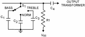
Figure 2-24. - Switch tone control.
Crystal Filters
A quartz crystal, used as a selective filter in the IF section of a communications
receiver, is one of the most effective methods of achieving maximum selectivity.
It is especially useful when the channel is crowded and considerable noise (both
external and internal) is present.
One possible circuit arrangement is shown in figure 2-25. Let's look at the theory
involved in understanding this circuit. You can see a crystal in one leg of the
bridge circuit. The secondary of the input transformer (T1) is balanced to ground
through the center tap connection. The crystal acts as a high Q series resonant
circuit. It allows signals within the immediate vicinity of resonance to pass through
the crystal to the output coil (L3). The desired signal appears between the center
tap of L3 and ground.
2-26
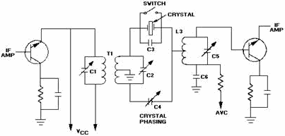
Figure 2-25. - Crystal filter used in the IF section of a superheterodyne receiver.
The capacitance that exists between the crystal holder plates (C3) may bypass
unwanted signals around the crystal; therefore, some method must be provided to
balance out this capacitance. You accomplish circuit balancing by applying out-of-phase
voltages to neutralize any undesired signal voltages. The tap on L3 permits proper
impedance matching and is the balanced input to the next stage.
Q23. What does a tone control circuit in a receiver do to the audio
signal?
Q24. What is the function of a crystal filter in a receiver?
Automatic Frequency Control
AFC circuits are used in situations where you must accurately control the frequency
of an oscillator by some external signal. Basically, this type circuit does two
things: It senses the difference between the actual oscillator frequency and the
frequency that is desired and produces a control voltage proportional to the difference;
it also uses the control voltage to change the oscillator to the desired frequency.
AFC circuits are used to control the frequency of sinusoidal oscillators and nonsinusoidal
oscillators. Only sinusoidal AFC circuits will be covered here. AFC circuits are used in radio receivers, fm transmitters, and frequency synthesizers to maintain
frequency stability. Figure 2-26 is a block diagram illustrating AFC operation in
a receiver. Let's run through the applicable parts of this block diagram.
2-27
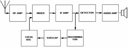
Figure 2-26. - Block diagram of receiver showing automatic frequency control.
The frequency discriminator controls the varicap in this receiver. a varicap
is used to keep the IF stable. You may want to review varicap theory in chapter
3 of NEETS, Module 7, Introduction to Solid- State Devices and Power Supplies at
this point. The varicap application here produces an apparent reactance, which is
included in the oscillator frequency control circuitry. For example, let's assume
the IF is 455 kilohertz and the local oscillator (lo) is tracking below the incoming
station. When the lo output decreases slightly in frequency, the IF will rise. This
causes the output of the discriminator to increase the capacitive reactance of the
varicap, which increases the oscillator frequency to the desired value. Now let's
assume the lo output increases. The IF will then decrease. This causes the discriminator
output to decrease the capacitive reactance of the varicap. This will cause the
oscillator frequency to decrease.
Figure 2-27 shows another widely used type of AFC and its circuitry. This type
is commonly referred to as a BALANCED-Phase DETECTOR or Phase-DIsCRIMINATOR. This
circuit uses fixed capacitors and the varying conductance of the diodes to achieve
a variable reactance. As you have seen in the block diagram, an AFC circuit requires
two sections, a frequency detector and a variable reactance. Our detector output
is a dc control voltage proportional to the amount of frequency change. This dc
voltage is applied directly to the oscillator. The phase inverter input signals
are discriminated IF outputs fed to the two diodes 180 degrees out of phase.
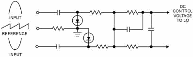
Figure 2-27. - Automatic frequency control (phase discriminator).
A reference voltage is also applied to both diodes. The diodes are biased to
conduct only during the peak portions of the input signals. Any change in oscillator
frequency will alter the phase relationship between the sawtooth reference voltage
and the incoming signals. If this happens, one diode will conduct
2-28
more than the other and produce a control signal. This system remains unbalanced
at all times because any change in frequency is instantaneously corrected. The network
between the diodes and oscillator is essentially a low-pass filter. This filter
prevents discriminator pulses from reaching the oscillator.
Frequency SYNTHESIs
In present day communications systems, long term accuracy of one part in a million
is required from many of the frequency generators (local oscillators) used in communications
equipment. Variable frequency oscillators cannot practically achieve this high degree
of stability. Therefore, a system known as Frequency SYNTHESIs has been developed
to meet the stringent demands for stability. This system uses circuitry that produces
a signal frequency through a heterodyning and frequency selection process. This
signal is not harmonically related to any of the signals used in the heterodyning
process. It is also not related to the selected crystal frequency. This makes the
signal unique.
Figure 2-28 is a multiple crystal, frequency synthesizer that produces desired
output frequencies by mixing frequencies from several crystal oscillators. Each
oscillator uses ten or more crystals to control its operating frequency. This provides
for a large number of output frequency combinations. Figure 2-29 is a practical
frequency synthesizer in which the harmonics and subharmonics of a single standard
oscillator are combined to provide a wide multichoice of output signals. Each of
these signals is harmonically related to a subharmonic of the standard oscillator.
You will find the primary difficulty encountered in the frequency synthesizers is
the presence of spurious signals generated in the "combining mixers." Extensive
filtering and extremely careful selection of operating frequencies are required
for even the simplest circuits. Spurious frequency problems increase and channel
spacing decreases as the range of operating frequencies increases.
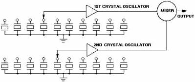
Figure 2-28. - Multiple crystal frequency synthesizer.
2-29
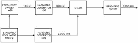
Figure 2-29. - Simple crystal frequency synthesizer.
Q25. What is the primary function of an AFC circuit?
Q26. What is frequency synthesis?
Audio REProductION DEVICES
The purpose of audio reproduction devices, such as loudspeakers and headphones,
is to convert electrical audio signals to sound power. Figure 2-30 shows you a diagram
of a loudspeaker called the PERMANENT MAGNET SPEAKER. This speaker consists of a
permanent magnet mounted on soft iron pole pieces, a voice coil that acts as an
electromagnet, and a loudspeaker cone connected to the voice coil. The audio signal
has been previously amplified (in terms of both voltage and power) and is applied
to the voice coil. The voice coil is mounted on the center portion of the soft iron
pole pieces in an air gap so that it is mechanically free to move. It is also connected
to the loudspeaker cone; as it moves, the cone will also move. When audio currents
flow through the voice coil, the coil moves back and forth proportionally to the
applied ac current. As the cone (diaphragm) is attached to the voice coil, it also
moves in accordance with the signal currents; in so doing, it periodically compresses
and rarefies the air, which produces sound waves.
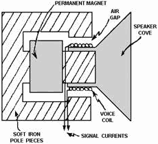
Figure 2-30. - Permanent magnet speaker.
2-30
|