|
October 1973 Popular Electronics
 Table of Contents Table of Contents
Wax nostalgic about and learn from the history of early electronics. See articles
from
Popular Electronics,
published October 1954 - April 1985. All copyrights are hereby acknowledged.
|
Mr. Lothar Stern, of
Motorola Semi, published a 3-part series on transistor theory in Popular Electronics
magazine in 1973. This is part 3.
Part 1 introduced the basics of the bipolar transistor, and
Part 2 addressed transistor circuit configurations - common emitter,
common gate, common collector, Darlington, differential - as well as presenting
gain equations and delving a bit into the physical construction of the semiconductor
elements. Finally, the author talks about the newest processes in use at the time
and what was available for low power and high power RF applications. In 1973, high
power semiconductors were just pushing past the 100 MHz barrier. Gallium arsenide
(GaAs) and gallium nitride (GaN) were still in university and corporate laboratories
being prepared for the amazing devices we have powering today's wireless products.
Here are Part 1,
Part 2, and
Part 3 (thanks to Jeff, KE5KQJ, for providing
a copy of Part 3).
Do You Know Your Bipolar Transistors? - Part 3
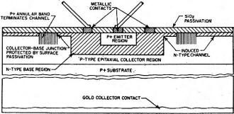
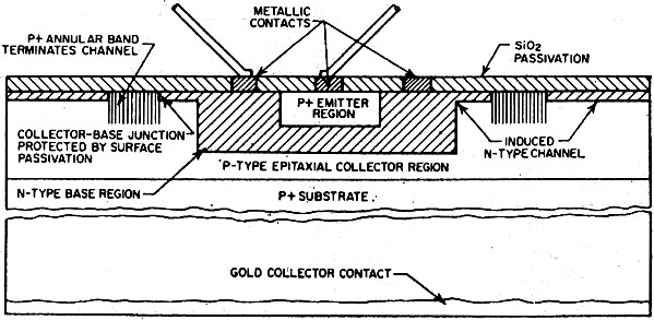
Fig. 15 - Latest process is epitaxial planar with annular
ring.
Conclusion of a 3-Part Series on Basic Transistor Theory
By Lothar Stern, Motorola Semiconductor Products Inc.
Newer Processes
Among new techniques, the latest process (see
Fig. 15) diffuses controlled-geometry base and emitter regions into the collector
layer and covers the entire device with a protective coating of silicon dioxide
to eliminate impurity contamination. It permits operation at extremely high frequency,
high voltage, and high current and provides good reliability at low cost.
For small-signal, low-frequency transistors, the epitaxial planar structure with
annular ring is, by far the most widely used. For high-power applications, however,
other processes are often employed to optimize characteristics needed for special
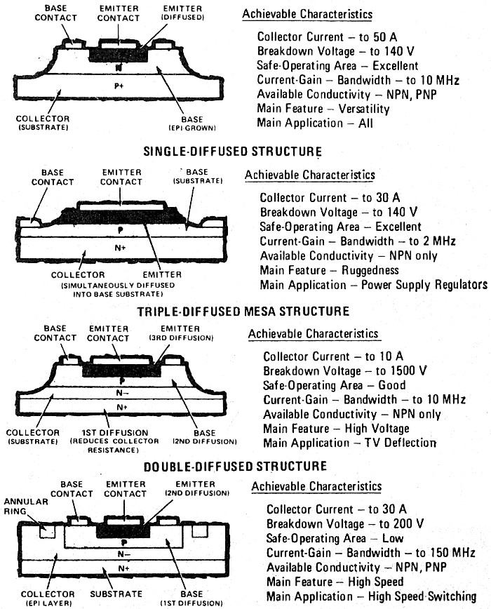
requirements. Figure 16 shows the most common power-transistor processes.
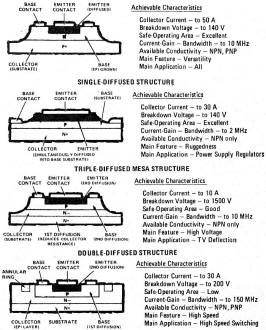
Fig. 16 - Cross sections of the processes employed in making
transistors for power applications, with some characteristics.
EPI-Base Structure, Single-Diffused Structure, Triple-Diffused
Mesa Structure, Double-Diffused Structure
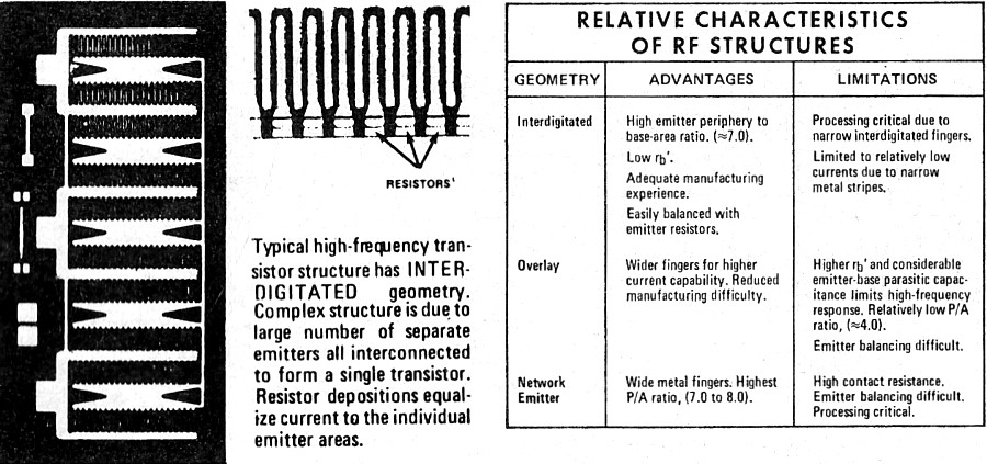
At very high frequencies, power transistors take on very complex geometries to
compensate for current crowding. The latter restricts the emission of charge carriers
to the edges of the emitter at high current levels. With rectangular or round emitters,
therefore, the center portion of the emitter does not contribute to current emission,
but it does add parasitic capacitance which reduces high-frequency response. High-frequency
structures, therefore, have very long, thin emitters which may be folded many times
to fit within a given base area. (Fig. 17) This greatly increases the ratio
of emitter periphery to base area, thereby maximizing the emission-to-capacitance
ratio. These extremely complex structures stress present processing technology to
its limits, accounting for the rapid increases in prices as frequency capabilities
of power transistors go beyond 100 MHz.
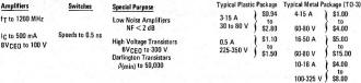
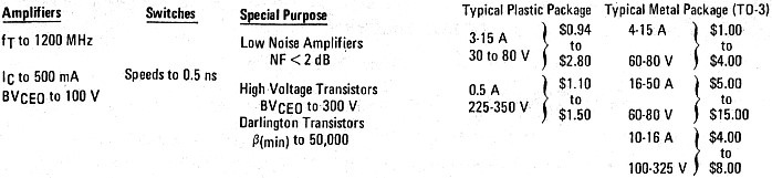
Table I - Small-signal transistor capabilities.
Typical high-frequency transistor structure has Inter-Digitated geometry. Complex
structure is due to large number of separate emitters all interconnected to form
a single transistor. Resistor depositions equalize current to the individual emitter
areas.
Table II - Low-frequency device capabilities
Transistor Capabilities
For small signal applications, today's
transistors cover virtually every conceivable requirement. Darlington (compound-connected)
transistors offer high input impedances and betas up to 75,000 at audio frequencies.
Amplifiers for r-f, oscillator, and mixer applications run well into the GHz band.
For special applications, low-noise transistors with noise figures around 2 dB are
common, and for high-voltage applications, devices with ratings up to several hundred
volts are no longer unique. And, due to plastic packaging, prices are so low that
there are few device capabilities that can't be purchased for under $1.00 even in
unit quantities, (See Table I.)
Low-Frequency Power
Power transistors for the lower frequencies
are also plentiful, but do not yet fill the desired applications as completely as
do the small-signal devices. (See Table II.). Prices are quite low for plastic packaged
devices rated up to 15 A and about 100 W. At currents below 5 A, even some of the
metal packaged devices are inexpensive. But prices rise rapidly at higher current
and voltage levels, particularly if higher frequency operation is required. Considerable
room for further development still exists.

Fig. 17. At very high frequencies, power transistors take
on some very complex geometries to compensate for current crowding. Characteristics
of structures are at right.
High-Frequency Power
At very high frequencies, the power picture
is still more limited. Power outputs of one to five watts are available up to 1
GHz, with up to 50 watts at 500 MHz and 100 watts in the 150-MHz region. Prices
remain high at the upper limits of power and frequency.

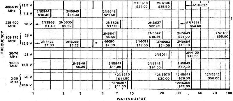
Fig. 18 - Range of transistor power available for given
frequency and supply voltage.
R-F Power
Figure 18 shows the range of transistor power commonly
available for a given frequency and power supply voltage. Specific device types
have been included to suggest possible choices for a particular application. The
power supply voltages given are those most usually encountered in practice. Devices
are tailored for best operation at these voltages. Using a transistor with a higher
than necessary voltage rating can result in performance degradation.
Posted July 9, 2024
(updated from original post
on 8/29/2018)
|