|
September 1973 Popular Electronics
 Table of Contents Table of Contents
Wax nostalgic about and learn from the history of early electronics. See articles
from
Popular Electronics,
published October 1954 - April 1985. All copyrights are hereby acknowledged.
|
Mr. Lothar Stern, of
Motorola Semi, published a 3-part series on transistor theory in Popular Electronics
magazine in 1973. This is part 2.
Part 1
introduced the basics of the bipolar transistor, and this follow-on article starts
addressing transistor circuit configurations - common emitter, common gate, common
collector, Darlington, differential - as well as presenting gain equations and delving
a bit into the physical construction of the semiconductor elements. Part 3
describes the newest processes in use at the time and what was available for low
power and high power RF applications.
Here are Part
1, Part
2, and Part
3 (thanks to Jeff, KE5KQJ, for providing a copy of Part 3).
Do You Know Your Bipolar Transistors? - Part 2
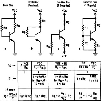
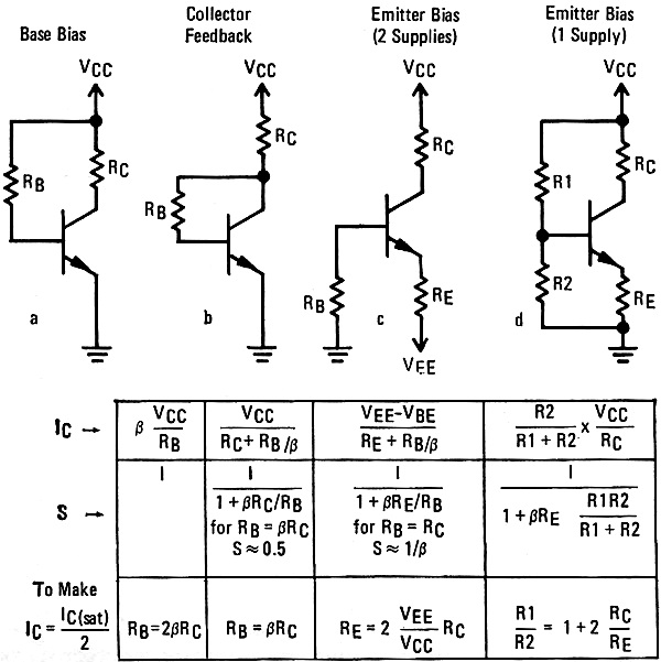
Fig. 5 - Conventional common-emitter bias circuits. Table
gives approximate characteristic expressions.
Part 2 of a 3-Part Series on Basic Transistor Theory
By Lothar Stern, Motorola Semiconductor Products Inc.
Biasing
When operated as an amplifier, the transistor must first be biased to some quiescent
value of collector current, so that both positive- and negative-going input voltage
excursions will cause corresponding changes in output voltage and current. The ideal
bias point is represented by Q on the loadline because this permits approximately
equal excursions in IC and VCE in both directions along the
load line without signal clipping. The bias point is established by a quiescent
base current that results in a dc collector current of approximately IC(sat)/2.
Several circuits are used for establishing the bias point. Among the most familiar
are those in Fig. 5. The basic performance difference is in the bias-point
stability. At point Q on the load line in Fig. 4, the transistor has a beta
of approximately 20. If a transistor with a beta of 40 were substituted (simulated
by dividing all IB values by 2), and if IB were held by the
bias circuit to 2.5 mA, as before, the operating point would move up the load line
to point Q', a much higher value of IC. As a result, considerable distortion
would occur for high-value input signals.

Fig. 6 - Circuit of a typical common-emitter RC-coupled
amplifier and its ac and dc loading curves.

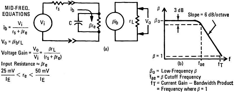
Fig. 7 - Equivalent high-frequency common-emitter circuit
(a) and its response (b).
Fig. 11 - Typical alloy transistor.
The bias point stability factor (S) is defined as the percent-change in IC,
for a percent-change in β, or ΔIC/IC = SΔβ/β.
If a percent-change of β causes a corresponding percent-change in IC,
the least desirable condition, then S = 1. If IC is independent of β
(corresponding to a zero change in IC when β is varied), then S
= O. The formulas accompanying Fig. 5 give IC and S as functions
of β and assign values for S under specific operating conditions. The bias arrangements
in Fig. 5c and 5d using emitter degeneration are preferred because, by proper
choice of resistor values, the effect of β on IC can be made almost
negligible. This prescribes a large value of RE, so that the voltage,
IERE, at the emitter is much larger than VBE or
IBRB. To prevent degenerative ac feedback, RE is
normally bypassed by a large-value capacitor. (Figure 5c is used when a positive
and negative power supply is available. For single-supply operation, Fig. 5d
is preferred.
In practical transistor amplifiers (RC coupled amplifier, for example) the operating
point is influenced by both dc and ac conditions. Figure 6 shows a typical RC-coupled
amplifier and its representative loadline plot. Note that there are two loadlines
- a dc loadline whose slope is affected only by the value of RC and an
ac loadline whose slope is determined by rL, the equivalent resistance
of RC and RL in parallel. The dc loadline represents the path
along which the operating point can be established. The ac loadline intersects the
dc loadline at the operating point, and the actual signal varies along the ac loadline,
which sets the V and I output limits.
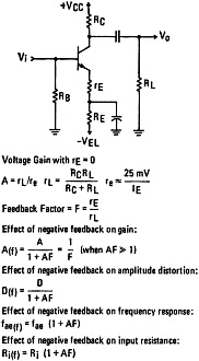
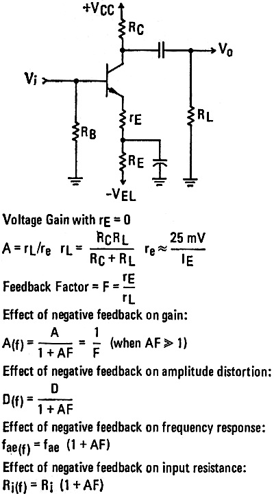
Fig. 8 - One-stage amplifier and equations for feedback
effects.

Fig. 9 - Darlington transistor pair.
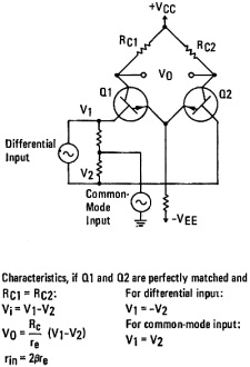
Fig. 10 - Basic differential amplifier.
The ac performance of the circuit in Fig. 6 can be established from the
high-frequency equivalent circuit in Fig. 7a. (For this approximation, it is
assumed that the signal frequencies are high enough that all capacitive reactances
of Fig. 6 are negligibly small.)
Each transistor junction has an associated junction capacitance. These are quite
small (on the order of a few picofarads), but they do affect transistor action at
high frequencies. A typical transistor frequency response plot is shown in Fig. 7b.
At the frequency where the reactance of the parasitic input capacitance equals the
input resistance, βre, the current to the input resistance is bypassed
through the capacitance to the point where the effective β is down 3 dB from
its low-frequency value. This is called the β-cutoff frequency, fae.
If the frequency is further increased, β continues to decrease at a rate of
6 dB per octave. The frequency at which β equals unity is specified on data
sheets as fT, the current-gain/bandwidth product. Given
fT, it is possible to determine transistor β for any frequency
between fae and fT from the relation β
= fT/f.
Negative Feedback. While the dc degenerative feedback associated
with RE of Fig. 6 stabilizes the operating point, making it independent of
changes in beta and other temperature-dependent parameters, the bypass capacitor
keeps it from compensating for the deleterious effects of these changes on the ac
signal. Moreover, while proper placement of the operating point can reduce non-symmetrical
signal clipping, it cannot reduce the distortion for large signal swings caused
by nonlinearity of the ICIB, characteristics (Fig. 4).
These characteristics can be greatly improved by means of negative signal feedback,
which requires a small unbypassed resistor, rE, in series with RE
as shown in Fig. 8. (This is only one of many possible feedback arrangements.)
In addition, negative feedback improves frequency response and compensates for changes
in output voltage (and gain) due to variations in temperature-sensitive parameters
such as re, and βac.
The equations accompanying Fig. 8 describe the basic advantages achieved
through negative feedback, as well as the price paid for them in terms of voltage
gain. However, since feedback increases input resistance, the loss of gain can partly
be recovered because of an increase in the gain of a previous stage caused by the
increase in input resistance.
Darlington Transistors
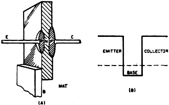
Fig. 12 - The microalloy structure.

Fig. 13 - Microalloy diffused type.

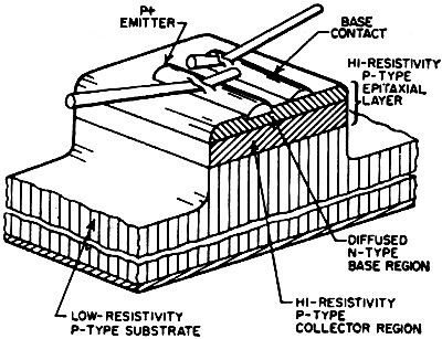
Fig. 14 - Epitaxial mesa structure.
Modern semiconductor technology not only has led to complete circuits on a single
chip of silicon (integrated circuits) but also to compound-connected transistors.
For the circuit designer, the latter provides some cost and space savings, while
still permitting unrestricted circuit design freedom. One of these devices is the
Darlington pair shown in Fig. 9.
Though consisting of two interconnected transistors, the device can actually
be treated as a single transistor with extremely high current gain and input resistance.
Normally, Darlington pairs are employed in the grounded collector configuration.
Commercially, they are available as small-signal and power devices, in both npn
and pnp polarities and with betas ranging from several 100 to several 1000.
Differential Amplifiers. With the advent of integrated circuits,
the circuit in Fig. 10 has become increasingly important. Being de coupled
through a common emitter resistor, it has no low-frequency limit; but, unlike other
types of dc-coupled amplifiers, it exhibits excellent stability and drift-free operation
without requiring elaborate compensating circuitry. This is its most important characteristic.
Operated in the differential mode, as shown, the output voltage responds only to
difference inputs to the two bases. If a common-mode signal were applied (as in
the case of ground line or power supply noise) or if the characteristics of the
transistors were to change in response to a change in temperature, the collector
current of both transistors would be affected equally. As a result, the output voltage
between the collectors would remain constant.
Transistor Fabrication Processes.
Over the years, many processes and structures have been used in transistor fabrication.
Most of them are still being used, though the older processes no longer offer the
best obtainable performance. The major sequential developments in the processing
of the bipolar transistor are shown in Figs. 11 through 15.
In Fig. 11A is a typical alloy transistor, while Fig. 11B shows its
impurity profile. It is simple and inexpensive to build. It provides excellent low-frequency
beta and can operate at high currents and power levels, but not at high frequencies
or high voltages.
Figure 12 shows the construction detail and impurity profile of a typical microalloy
(MAT) structure. It is similar to the technique shown in Fig. 11 except that
shallow pits are etched into the base substrate prior to collector and emitter alloying.
The thinner base improves the frequency response but results in a fragile structure
and further reduces breakdown voltage.
The process shown in Fig. 13 uses diffusion of impurities into a thin base
membrane prior to alloying to permit a closely controlled, graded impurity profile.
This technique offers frequency responses up to 100 MHz.
The process shown in Fig. 14, with extremely thin collector and base regions
and unrestricted use of different material resistivities, provides high-frequency
performance up to a gigahertz. It also provides high gain and high breakdown voltage.
However, sensitive pn junctions are exposed to the atmosphere, resulting in high
leakage current.
Posted January 19, 2024
(updated from original
post on 9/7/2017)
|