|
August 1970 Popular Electronics
 Table
of Contents Table
of Contents
Wax nostalgic about and learn from the history of early electronics. See articles
from
Popular Electronics,
published October 1954 - April 1985. All copyrights are hereby acknowledged.
|
Beginning in the 1960s,
Popular Electronics magazine had a long-running column titled "Solid State"
that reported on the newfangled science. Even in 1970, there were still people who
distrusted solid state electronic devices in terms of reliability and ruggedness.
Their skepticisms were not totally without merit at the time. However, advances
were occurring at a very rapid rate. This particular Solid State report describes
how charge coupled devices (CCD) might someday serve as photographic imagers because
of their efficiency at converting photon impingement to electric charge in potential
wells and the subsequent serial shifting of the data to an output port. It also
raves at the development by Motorola of RF power transistors (40 W) that exhibited
useful gain way up into the 25 MHz realm.
Solid State columns: April 1967,
August 1967,
April 1966,
August 1970,
July 1971,
October 1971,
April 1972.
Solid State
By Lou Garner, Semiconductor Editor
New Technique Lowers Cost
 Employing principles never before used in semiconductor
technology, scientists at the Bell Telephone Laboratories have created a new class
of low-cost, reliable electronic devices suitable for use in logic, imaging, and
memory applications. Dubbed Charge Coupled Devices (CCD's), the new units perform
many of the functions of more complex integrated circuits, yet are simple and easily
fabricated. Employing principles never before used in semiconductor
technology, scientists at the Bell Telephone Laboratories have created a new class
of low-cost, reliable electronic devices suitable for use in logic, imaging, and
memory applications. Dubbed Charge Coupled Devices (CCD's), the new units perform
many of the functions of more complex integrated circuits, yet are simple and easily
fabricated.
As illustrated in Fig. 1, a typical CCD structure consists of three layers:
metal conductors, an insulating layer of silicon dioxide, and a base of homogeneous
silicon semiconductor material. The basic technology is applicable to a wide range
of semiconductor-insulator systems, however, and is not restricted just to those
materials in which it is possible to form p-n junctions.
A CCD creates and stores minority carriers (electrons or holes) in spatially
defined depletion regions called "potential wells" near the surface of the semiconductor.
In Fig. 1, an n-type semiconductor is used and the minority carriers are holes
at the semiconductor-insulator interface.
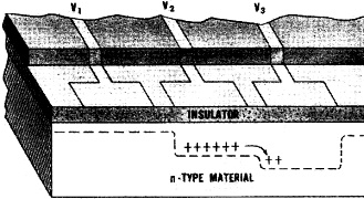
Fig. 1 - A CCD structure consists of three layers: metal
conductors (V1-v3), insulating layer of silicon dioxide, and base of homogeneous
silicon semiconductor material.
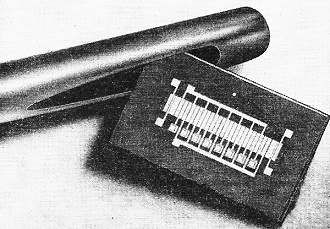
Fig. 2 - Experimental CCD 8-bit shift register shown in
photo is so small, it can be passed through eye of needle.
In operation, the potential wells are produced and moved by an array of metallic
electrodes. The electrodes normally are made negative with respect to the semiconductor
base. When voltage is first applied, there are no holes at the interface and the
potential is divided between the semiconductor and insulator. Holes introduced in
the depletion region by avalanche multiplication, or other means, collect at the
interface causing the potential to become more positive. The minority carriers forming
the potential wells may be moved from under one electrode to an adjacent electrode
on the same substrate by applying a more negative voltage to the adjacent electrode.
The sequence may be repeated, as needed, to move the carriers (and wells) in any
desired direction. When required, the resulting charge pattern can be detected and
measured by other electrodes.
Although still in its developmental stage, the CCD technology already has been
used to fabricate a number of useful devices, including the experimental 8-bit shift
register illustrated in Fig. 2. Future units may include other logic and switching
devices as well as CCD image sensors, in which potential well patterns would be
created through photoelectric action by light images focused on the back side of
the semiconductor substrate, then read out using the metal electrodes.
Reader's Circuit. The sequential lamp control circuit of Fig. 3
was submitted by reader Paul Schultz (6208 Templeton Drive, Carmichael, CA 95608).
If coupled to a conventional electromechanical or thermal flasher switch, it can
be used as an automotive sequential-type directional turn signal. In addition, the
basic circuit can be employed in moving-light advertising displays, in warning systems,
and in other similar applications.
In operation, lamp I1 lights as soon as power is applied. Meanwhile, C1 is charged
slowly through R1 and R2, eventually firing Q1 and developing a voltage pulse across
load resistor R4, which triggers SCR1 on, lighting lamp 12. With SCR1 on, C2 is
charged through R3 and R4, firing Q2, which triggers SCR2, lighting lamp I3. The
three lamps remain lit until circuit power is interrupted and restored by the external
flasher switch, at which time the cycle repeats. The lamps are ordinary 12-volt
automotive bulbs.
With neither layout nor lead dress critical, the builder can duplicate the project
using any construction technique. Although not essential in most applications, heat
sinks can be provided for the two SCR's as a precaution against overheating.
Two complete units are required, of course, for automotive turn-signal applications.
Usually, the controls can be mounted in the car's luggage compartment. After installation,
sequence timing resistors R2 and R4 must be adjusted for optimum performance in
conjunction with the car's regular flashing switch (that is, so that the full sequence
is completed during each flashing interval). If the control unit is used in non-automotive
service, these timing controls are adjusted to achieve the preferred display effect.
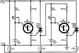
Fig. 3 - If coupled to conventional electromechanical or
thermal flasher switch, circuit shown can be used as auto sequential-type turn signal.
Device Developments. Four new types have been added to Motorola's
exclusive line of silicon pnp r.f. power transistors. Identified as types MM4020
through MM4023, the new devices offer output power ratings ranging from 3.5 to 40.0
watts, with gains from 11.5 to 4.5 dB. Designed for 12.5-volt VHF large-signal amplifier
applications at frequencies up to 20 MHz, the new transistors feature balanced emitter
construction in which thin-film nichrome resistors are in series with each of the
multiple emitters to distribute power evenly throughout the chip. This technique
prevents "hot emitters" and results in rugged devices which stand up under the high
voltage standing-wave-ratio conditions sometimes occurring in mistuned r.f. systems.
All four devices are supplied in strip-line packages with minimum series lead inductances.
For complete specifications, contact the Technical Information Center, Motorola
Semiconductor Products, Inc., Box 20924, Phoenix, AZ 85036.
Motorola also has introduced a new series of silicon power Darlington devices.
In a monolithic construction, both transistors and their compensating emitter resistors
make up the configuration on a single chip. The new units offer minimum d.c. betas
of 1,000 at VCEO ratings of 60 and 80 volts. Type numbers are MJ900 and MJ901 for
the pnp units and MJ1000 and MJ1001 for npn.
A new crystal-controlled microcircuit oscillator has been announced by TRW Semiconductors
(14520 Aviation Blvd., Lawndale, CA 90260). The new unit model, MCOF, operates in
the 5-MHz to 25-MHz frequency range, offering a frequency stability of 0.003% from
-55°C. to 125°C. Contained in a 4-lead TO-5 package, the device uses thin-film
capacitors and resistors on a single substrate and is designed specifically for
applications as the local oscillator for the second mixer in dual conversion receivers.
Operating voltage is 1.8 to 5.0 volts, while the output ranges from 0.35 to 3.0
volts r.m.s. into a 1,000-ohm load.
Practical Publications. A cross reference guide of IR universal
replacement transistors and rectifiers is now available from International Rectifier's
Semiconductor Division. Folding to a handy 3" x 5 1/2" size, small enough to fit
a shirt pocket, the booklet lists IR types corresponding to devices offered by Motorola,
GE, RCA, Sylvania, Delco and Tungsol, covering the most popular transistors and
rectifiers used in professional servicing, hobby projects, and technical experiments.
In addition, transistor and rectifier specifications for all the IR devices listed
are presented in easy-to-use tabular form. For your copy of this informative guide,
write to International Rectifier, Semiconductor Division, Dept. 781, 233 Kansas
Street, EI Segundo, CA 90245.
Texas Instruments, Inc. (P. O. Box 5012, Dallas, TX 75222) has recently published
an extremely useful 8-page booklet entitled the Design Assistance Directory, Bulletin
CM-102C. Listing a wide range of literature resources covering solid-state circuit
applications and design techniques, the publication includes abstracts describing
textbooks, brochures, catalogs, and application reports.
Transitips. A common problem facing the serious hobbyist is
that of improving or modifying the performance of an existing circuit design. While
space limitations prohibit an exhaustive discussion of all available techniques,
we'll try to cover various aspects of the problem from time to time - starting,
this month, with a look at the techniques for extending the low frequency response
of an R-C coupled amplifier.
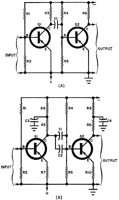
Consider, first, the basic two-stage amplifier circuit illustrated in Fig. 4A.
Here, voltage-dividers R1-R2 and R4-RS establish base biases for Q1 and Q2, respectively,
while R3 and R6 serve as corresponding collector loads. Capacitor C1 provides inter-stage
coupling.
The important factors affecting the circuit's low-frequency response are the
size of the coupling capacitor (C1) and the input impedance of the following stage.
In practice, the coupling device and the input impedance form a frequency-sensitive
voltage divider.
One technique for extending the low-frequency response is simply to use a larger-valued
coupling capacitor - either substituting another unit, or connecting a second capacitor
in parallel with the first, as C2 in Fig.4B.

Fig. 4 - Low-frequency response of amplifier shown at (A)
can be improved by changes shown in (8) circuit.
Another technique is to raise the effective input impedance of each stage. This
can be accomplished at a loss in overall gain by adding unbypassed emitter resistances,
as R7 and R10 in Fig. 4B. The value of the resistors used will vary considerably
from one circuit to another but, in general, will range from a few ohms in the case
of power transistors (or even a fraction of an ohm for multi-watt stages) to as
high as several hundred ohms where low-signal levels are involved.
A final technique, commonly used in oscilloscopes and some instrument amplifiers,
is the use of a low-frequency "boost" network. In general, this takes the form of
a simple L-type circuit, as illustrated by C3-R8 and C4-R9 in Fig. 4B. At the
same time, somewhat smaller main load resistors (R3 and R6) are used. The net effect
is to establish a frequency-sensitive load which raises the stage's effective gain
at low frequencies.
In the first stage (Q1), for example, R3 serves as the prime collector load at
mid-range and high frequencies, because C3 acts as an effective mid-to-high frequency
bypass device. As lower frequencies are approached, C3's impedance increases and
R8 becomes a part of the collector load. The lower the frequency, the higher the
load impedance and the greater the stage's gain.
The component values needed will vary considerably with the specific circuit
parameters. Generally speaking, however, the prime load resistor (R3) might be reduced
to two-thirds or one-half of its original value, with the secondary load (R8) making
up the difference. The boost capacitor (C3) may range in value from one to as high
as 20 μF depending on the amount of boost needed.
That's it for August - until next month, keep boosting!
- Lou
Posted March 19, 2024
(updated from original post
on 6/27/2017)
|